M25P128 데이터 시트보기 (PDF) - STMicroelectronics
부품명
상세내역
제조사
M25P128
STMicroelectronics

M25P128 Datasheet PDF : 45 Pages
| |||
SPI modes
3
SPI modes
M25P128
These devices can be driven by a microcontroller with its SPI peripheral running in either of
the two following modes:
● CPOL=0, CPHA=0
● CPOL=1, CPHA=1
For these two modes, input data is latched in on the rising edge of Serial Clock (C), and
output data is available from the falling edge of Serial Clock (C).
The difference between the two modes, as shown in Figure 5, is the clock polarity when the
bus master is in Stand-by mode and not transferring data:
● C remains at 0 for (CPOL=0, CPHA=0)
● C remains at 1 for (CPOL=1, CPHA=1)
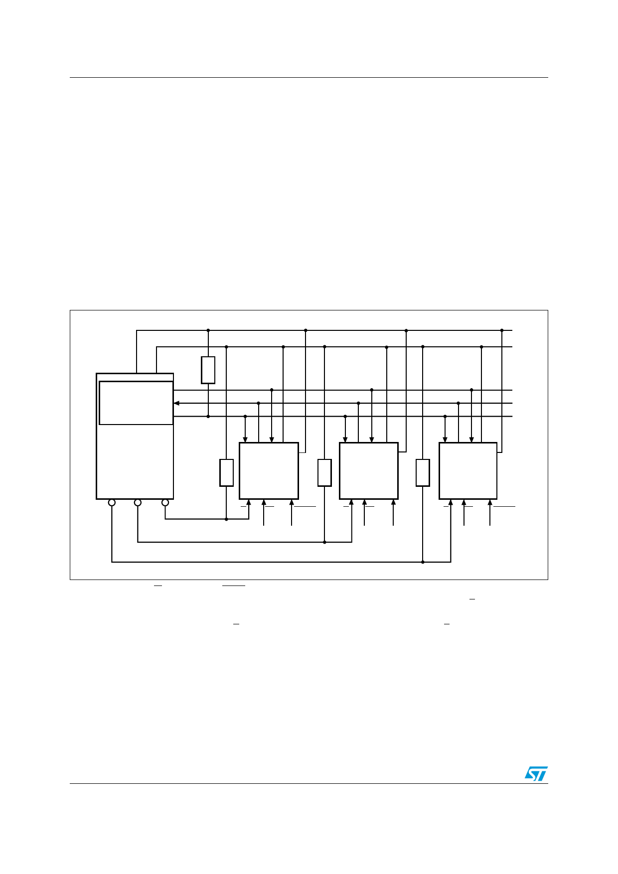
Figure 4. Bus master and memory devices on the SPI bus
SPI Interface with
(CPOL, CPHA) =
(0, 0) or (1, 1)
R(2)
SDO
SDI
SCK
SPI bus master
R(2)
CS3 CS2 CS1
VSS
VCC
CQD
VCC
VSS
CQD
VCC
VSS
C Q D VCC
VSS
SPI memory R(2)
device
SPI memory R(2)
device
SPI memory
device
S
W/VPP HOLD
S W/VPP HOLD
S W/VPP HOLD
AI12836
1. The Write Protect (W/VPP) and Hold (HOLD) signals should be driven, High or Low as appropriate.
2. These pull-up resistors, R, ensure that the memory devices are not selected if the Bus Master leaves the S line in the high-
impedance state. As the Bus Master may enter a state where all inputs/outputs are in high impedance at the same time
(e.g.: when the Bus Master is reset), the clock line (C) must be connected to an external pull-down resistor so that, when all
inputs/outputs become high impedance, S is pulled High while C is pulled Low (thus ensuring that S and C do not become
High at the same time, and so, that the tSHCH requirement is met).
10/45
Share Link: