M25P80-VMW3 데이터 시트보기 (PDF) - STMicroelectronics
부품명
상세내역
제조사
M25P80-VMW3 Datasheet PDF : 41 Pages
| |||
M25P80
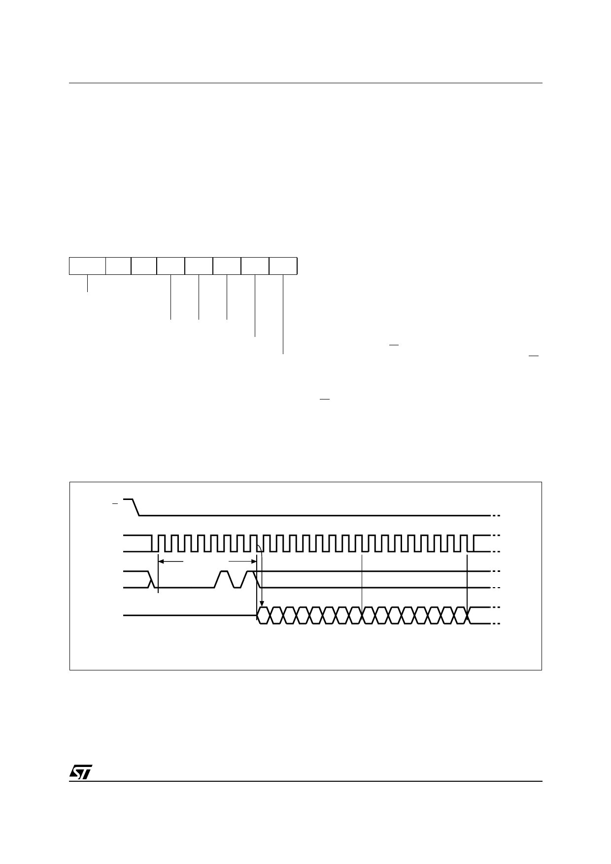
Read Status Register (RDSR)
The Read Status Register (RDSR) instruction al-
lows the Status Register to be read. The Status
Register may be read at any time, even while a
Program, Erase or Write Status Register cycle is in
progress. When one of these cycles is in progress,
it is recommended to check the Write In Progress
(WIP) bit before sending a new instruction to the
device. It is also possible to read the Status Reg-
ister continuously, as shown in Figure 11..
Table 5. Status Register Format
b7
b0
SRWD 0 0 BP2 BP1 BP0 WEL WIP
Status Register
Write Protect
Block Protect Bits
Write Enable Latch Bit
Write In Progress Bit
The status and control bits of the Status Register
are as follows:
WIP bit. The Write In Progress (WIP) bit indicates
whether the memory is busy with a Write Status
Register, Program or Erase cycle. When set to 1,
such a cycle is in progress, when reset to 0 no
such cycle is in progress.
WEL bit. The Write Enable Latch (WEL) bit indi-
cates the status of the internal Write Enable Latch.
When set to 1 the internal Write Enable Latch is
set, when set to 0 the internal Write Enable Latch
is reset and no Write Status Register, Program or
Erase instruction is accepted.
BP2, BP1, BP0 bits. The Block Protect (BP2,
BP1, BP0) bits are non-volatile. They define the
size of the area to be software protected against
Program and Erase instructions. These bits are
written with the Write Status Register (WRSR) in-
struction. When one or both of the Block Protect
(BP2, BP1, BP0) bits is set to 1, the relevant mem-
ory area (as defined in Table 2.) becomes protect-
ed against Page Program (PP) and Sector Erase
(SE) instructions. The Block Protect (BP2, BP1,
BP0) bits can be written provided that the Hard-
ware Protected mode has not been set. The Bulk
Erase (BE) instruction is executed if, and only if,
both Block Protect (BP2, BP1, BP0) bits are 0.
SRWD bit. The Status Register Write Disable
(SRWD) bit is operated in conjunction with the
Write Protect (W) signal. The Status Register
Write Disable (SRWD) bit and Write Protect (W)
signal allow the device to be put in the Hardware
Protected mode (when the Status Register Write
Disable (SRWD) bit is set to 1, and Write Protect
(W) is driven Low). In this mode, the non-volatile
bits of the Status Register (SRWD, BP2, BP1,
BP0) become read-only bits and the Write Status
Register (WRSR) instruction is no longer accepted
for execution.
Figure 11. Read Status Register (RDSR) Instruction Sequence and Data-Out Sequence
S
0 1 2 3 4 5 6 7 8 9 10 11 12 13 14 15
C
Instruction
D
Status Register Out
Status Register Out
High Impedance
Q
76543210765432107
MSB
MSB
AI02031E
15/41
Share Link: 