X28LC512 데이터 시트보기 (PDF) - Xicor -> Intersil
부품명
상세내역
제조사
X28LC512 Datasheet PDF : 19 Pages
| |||
X28LC512/X28LC513
PIN DESCRIPTIONS
Addresses (A0–A15)
The Address inputs select an 8-bit memory location
during a read or write operation.
Chip Enable (CE)
The Chip Enable input must be LOW to enable all read/
write operations. When CE is HIGH, power consumption
is reduced.
Output Enable (OE)
The Output Enable input controls the data output buffers
and is used to initiate read operations.
Data In/Data Out (I/O0–I/O7)
Data is written to or read from the X28LC512/513
through the I/O pins.
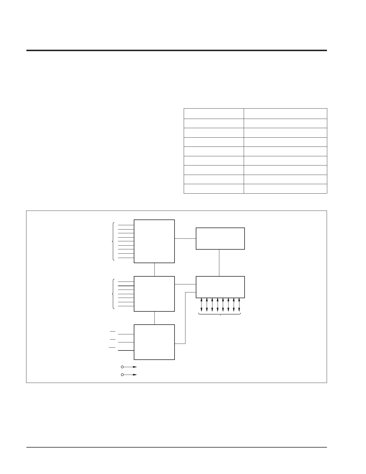
FUNCTIONAL DIAGRAM
Write Enable (WE)
The Write Enable input controls the writing of data to the
X28LC512/513.
PIN NAMES
Symbol
A0–A15
I/O0–I/O7
WE
CE
OE
VCC
VSS
NC
Description
Address Inputs
Data Input/Output
Write Enable
Chip Enable
Output Enable
3.3V ± 10%
Ground
No Connect
3005 PGM T01
A7–A15
X BUFFERS
LATCHES AND
DECODER
512K-BIT
E2PROM
ARRAY
A0–A6
Y BUFFERS
LATCHES AND
DECODER
CE
OE
WE
VCC
VSS
CONTROL
LOGIC AND
TIMING
I/O BUFFERS
AND LATCHES
I/O0–I/O7
DATA INPUTS/OUTPUTS
3005 ILL F01
2
Share Link: 