M28W320CT09GB1T 데이터 시트보기 (PDF) - STMicroelectronics
부품명
상세내역
제조사
M28W320CT09GB1T Datasheet PDF : 42 Pages
| |||
M28W320CT, M28W320CB
DEVICE OPERATIONS
Four control pins rule the hardware access to the
Flash memory: E, G, W, RP. The following opera-
tions can be performed using the appropriate bus
cycles: Read, Write the Command of an Instruc-
tion, Output Disable, Stand-by, Reset (see Table
5).
Read. Read operations are used to output the
contents of the Memory Array, the Electronic Sig-
nature, the Status Register and the CFI. Both Chip
Enable (E) and Output Enable (G) must be at VIL
in order to perform the read operation. The Chip
Enable input should be used to enable the device.
Output Enable should be used to gate data onto
the output independently of the device selection.
The data read depend on the previous command
written to the memory (see instructions RD, RSIG,
RSR, RCFI). Read Array is the default state of the
device when exiting reset or after power-up.
Write. Write operations are used to give Com-
mands to the memory or to latch Input Data to be
programmed. A write operation is initiated when
Chip Enable E and Write Enable W are at VIL with
Output Enable G at VIH. Commands, Input Data
and Addresses are latched on the rising edge of W
or E, whichever occur first.
Output Disable. The data outputs are high im-
pedance when the Output Enable G is at VIH.
Stand-by. Stand-by disables most of the internal
circuitry allowing a substantial reduction of the cur-
rent consumption. The memory is in stand-by
when Chip Enable E is at VIH and the device is in
read mode. The power consumption is reduced to
the stand-by level and the outputs are set to high
impedance, independently from the Output Enable
G or Write Enable W inputs. If E switches to VIH
during program or erase operation, the device en-
ters in stand-by when finished.
Reset. During Reset mode all internal circuits are
switched off, the memory is deselected and the
outputs are put in high impedance. The memory is
in Reset mode when RP is at VIL. The power con-
sumption is reduced to the stand-by level, inde-
pendently from the Chip Enable E, Out-put Enable
G or Write Enable W inputs. If RP is pulled to VSS
during a Program or Erase, this operation is abort-
ed and the memory content is no longer valid as it
has been compromised by the aborted operation.
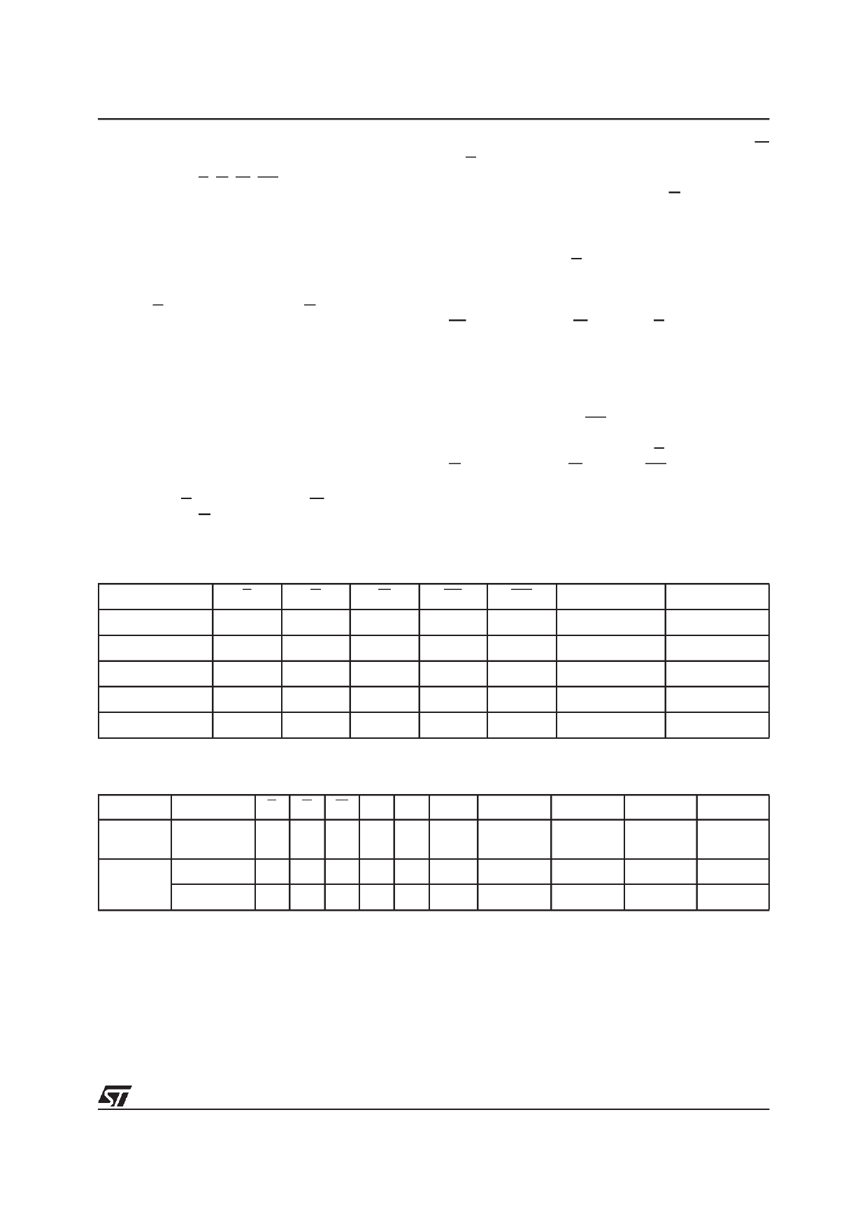
Table 5. User Bus Operations (1)
Operation
E
G
W
RP
WP
VPP
DQ0-DQ15
Read
VIL
VIL
VIH
VIH
X
Don’t Care
Data Output
Write
VIL
VIH
VIL
VIH
X
VDD or VPPH
Data Input
Output Disable
VIL
VIH
VIH
VIH
X
Don’t Care
Hi-Z
Stand-by
VIH
X
X
VIH
X
Don’t Care
Hi-Z
Reset
X
X
X
VIL
X
Don’t Care
Hi-Z
Note: 1. X = VIL or VIH, VPPH = 12V ± 5%.
Table 6. Read Electronic Signature (RSIG Instruction)
Code
Device
E G W A0 A1 A2-A7 A8-A11 A12-A20 DQ0-DQ7 DQ8-DQ15
Manufact.
Code
VIL VIL VIH VIL VIL
0 Don’t Care Don’t Care
20h
00h
Device
M28W320CT VIL VIL VIH VIH VIL
0 Don’t Care Don’t Care
BAh
88h
Code
M28W320CB VIL VIL VIH VIH VIL
0 Don’t Care Don’t Care
BBh
88h
7/42
Share Link: 