M29W160 데이터 시트보기 (PDF) - STMicroelectronics
부품명
상세내역
제조사
M29W160
STMicroelectronics

M29W160 Datasheet PDF : 25 Pages
| |||
M29W160BT, M29W160BB
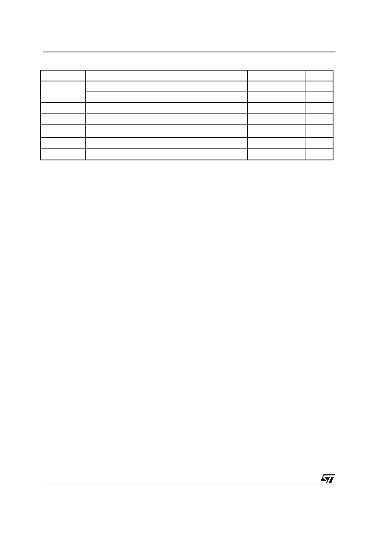
Table 2. Absolute Maximum Ratings (1)
Symbol
Parameter
Value
Unit
Ambient Operating Temperature (Temperature Range Option 1)
0 to 70
°C
TA
Ambient Operating Temperature (Temperature Range Option 6)
–40 to 85
°C
TBIAS
Temperature Under Bias
–50 to 125
°C
TSTG
Storage Temperature
–65 to 150
°C
VIO (2)
Input or Output Voltage
–0.6 to 4
V
VCC
Supply Voltage
–0.6 to 4
V
VID
Identification Voltage
–0.6 to 13.5
V
Note: 1. Except for the rating ”Operating Temperature Range”, stresses above those listed in the Table ”Absolute Maximum Ratings” may
cause permanent damage to the device. These are stress ratings only and operation of the device at these or any other conditions
above those indicated in the Operating sections of this specification is not implied. Exposure to Absolute Maximum Rating condi-
tions for extended periods may affect device reliability. Refer also to the STMicroelectronics SURE Program and other relevant qual-
ity documents.
2. Minimum Voltage may undershoot to –2V during transition and for less than 20ns during transitions.
SUMMARY DESCRIPTION
The M29W160B is a 16 Mbit (2Mb x8 or 1Mb x16)
non-volatile memory that can be read, erased and
reprogrammed. These operations can be per-
formed using a single low voltage (2.7 to 3.6V)
supply. On power-up the memory defaults to its
Read mode where it can be read in the same way
as a ROM or EPROM.
The memory is divided into blocks that can be
erased independently so it is possible to preserve
valid data while old data is erased. Each block can
be protected independently to prevent accidental
Program or Erase commands from modifying the
memory. Program and Erase commands are writ-
ten to the Command Interface of the memory. An
on-chip Program/Erase Controller simplifies the
process of programming or erasing the memory by
taking care of all of the special operations that are
required to update the memory contents.
The end of a program or erase operation can be
detected and any error conditions identified. The
command set required to control the memory is
consistent with JEDEC standards.
The blocks in the memory are asymmetrically ar-
ranged, see Tables 3 and 4, Block Addresses. The
first or last 64 Kbytes have been divided into four
additional blocks. The 16 Kbyte Boot Block can be
used for small initialization code to start the micro-
processor, the two 8 Kbyte Parameter Blocks can
be used for parameter storage and the remaining
32K is a small Main Block where the application
may be stored.
Chip Enable, Output Enable and Write Enable sig-
nals control the bus operation of the memory.
They allow simple connection to most micropro-
cessors, often without additional logic.
The memory is offered in TSOP48 (12 x 20mm),
SO44 and LFBGA48 (0.8mm pitch) packages and
it is supplied with all the bits erased (set to ’1’).
4/25
Share Link: