EL2008C 데이터 시트보기 (PDF) - Elantec -> Intersil
부품명
상세내역
제조사
EL2008C Datasheet PDF : 12 Pages
| |||
EL2008C
55 MHz 1 Amp Buffer Amplifier
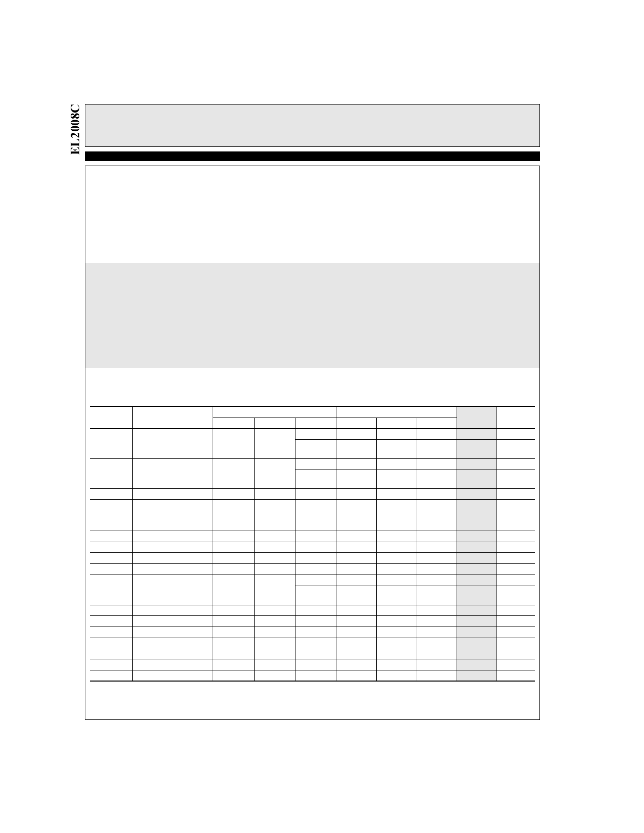
Absolute Maximum Ratings (TA = 25°C)
VS
Supply Voltage (V+ - V-)
±18V or 36V
VIN
Input Voltage
±15 or VS
If the input exceeds the ratings shown (or the supplies) or if the input voltage exceeds ±7.5V
then the input current must be limited to ±50 mA. See the application hints for information.
IIN
Input Current (See note above)
±50 mA
PD
Power Dissipation
See Curves
The maximum power dissipation depends on package type, ambient temperature and heat
sinking. See the characteristic curves for more details.
TA
Operating Temperature Range
0°C to +75°C
TJ
Operating Junction Temp
175°C
TST
Storage Temp Range
-65°C to +150°C
TLD
Lead Solder Temp <10 seconds
300°C
Important Note:
All parameters having Min/Max specifications are guaranteed. The Test Level column indicates the specific device testing actually performed during
production and Quality inspection. Elantec performs most electrical tests using modern high-speed automatic test equipment, specifically the LTX77
Series system. Unless otherwise noted, all tests are pulsed tests, therefor TJ = TC = TA.
Test Level Test Procedure
I
100% production tested and QA sample tested per QA test plan QCX0002.
II
100% production tested at TA = 25°C and QA sample tested at TA = 25°C, TMAX and TMIN per QA test plan QCX0002.
III
QA sample tested per QA test plan QCX0002.
IV
Parameter is guaranteed (but not tested) by Design and Characterization Data.
V
Parameter is typical value at TA = 25°C for information purposes only.
Electrical Characteristics
VS = ±15V, RS = 50Ω, unless otherwise specified
Parameter
Description
VIN
VOS
Output Offset Voltage
0
Test Conditions
Load
×
IIN
Input Current
0
×
RIN
Input Impedance
±12V
100Ω
AV1
Voltage Gain
±10V
×
AV2
Voltage Gain
±10V
10Ω
AV3
Voltage Gain, VS = ±15V
±3V
10Ω
V01
Output Voltage Swing
±14V
100Ω
V02
Output Voltage Swing
±12V
10Ω
R01
Output Impedance
±10V
±10 mA
R02
Output Impedance
IO
Output Current
±10V
±1A
±12V
[1]
IS
PSRR
VS+, VS-
SR1
SR2
tr, tf
Supply Current
Supply Rejection [2]
Supply Sensitivity [3]
Slew Rate [4]
Slew Rate [5]
Rise/Fall Time
0
×
0
×
×
±10V
50Ω
±10V
10Ω
±5V
10Ω
100 mV
10Ω
Temp
25°C
TMIN,
TMAX
25°C
TMIN,
TMAX
25°C
25°C
25°C
25°C
25°C
25°C
25°C
25°C
25°C
TMIN,
TMAX
25°C
25°C
25°C
25°C
25°C
25°C
25°C
Min
-40
-50
-35
-50
0.5
0.985
0.88
0.87
±13
±10.5
1.25
1
12
60
Limits
Typ
10
-5
2
0.9995
0.91
0.89
±11
1.8
0.8
1.8
17
2500
1500
800
7
Max
Test Level Units
+40
I
mV
+50
IV
mV
+35
I
µA
+50
IV
µA
I
MΩ
I
V/V
I
V/V
I
V/V
I
V
I
V
2.5
I
Ω
1.15
I
Ω
I
A
IV
A
26
I
mA
I
dB
2
I
mV/V
V
V/µs
V
V/µs
V
V/µs
V
ns
2
Share Link: 