M5450 데이터 시트보기 (PDF) - STMicroelectronics
부품명
상세내역
제조사
M5450 Datasheet PDF : 12 Pages
| |||
M5450, M5451
Table 2. Static Electrical Characteristics
(Tamb within operating range, VDD = 4.75V to 13.2V, VSS = 0V, unless otherwise specified)
Symbol
Parameter
Test Conditions
Min. Typ. Max.
VDD Supply Voltage
4.75
13.2
IDD
Supply Current
VDD = 13.2V
7
VI
Input Voltage Logical "0" Level ± 10µA Input Bias
Logical "1" Level
4.75 ≤ VDD ≤ 5.25
- 0.3
2.2
0.8
VDD
VDD > 5.25
VDD - 2
VDD
IB
Brightness Input Current (note 2)
0
0.75
VB
Brightness Input Voltage (pin 19) Input Current = 750µA, Tamb = 25°C 3
4.3
VO(off) Off State Out. Voltage
13.2
IO
Out. Sink Current (note 3)
Segment OFF
VO = 3V
10
Segment ON
VO = 1V (note 4)
Brightness In. = 0µA
0
10
Brightness In. = 100µ
2
27
4
Brightness In. = 750µA
12
15 25
fclock Input Clock Frequency
0
0.5
IO
Output Matching (note 1)
± 20
Note: 1. Output matching is calculated as the percent variation from I MAX + IMIN/2.
2. With a fixed resistor on the brightness input some variation in brightness will occur from one device to another.
3. Absolute maximum for each output should be limited to 40mA.
4. The VO voltage should be regulated by the user. See Figure 7 and Figure 8 for allowable VO versus IO operation.
Unit
V
mA
V
V
V
mA
V
V
µA
µA
mA
mA
MHz
%
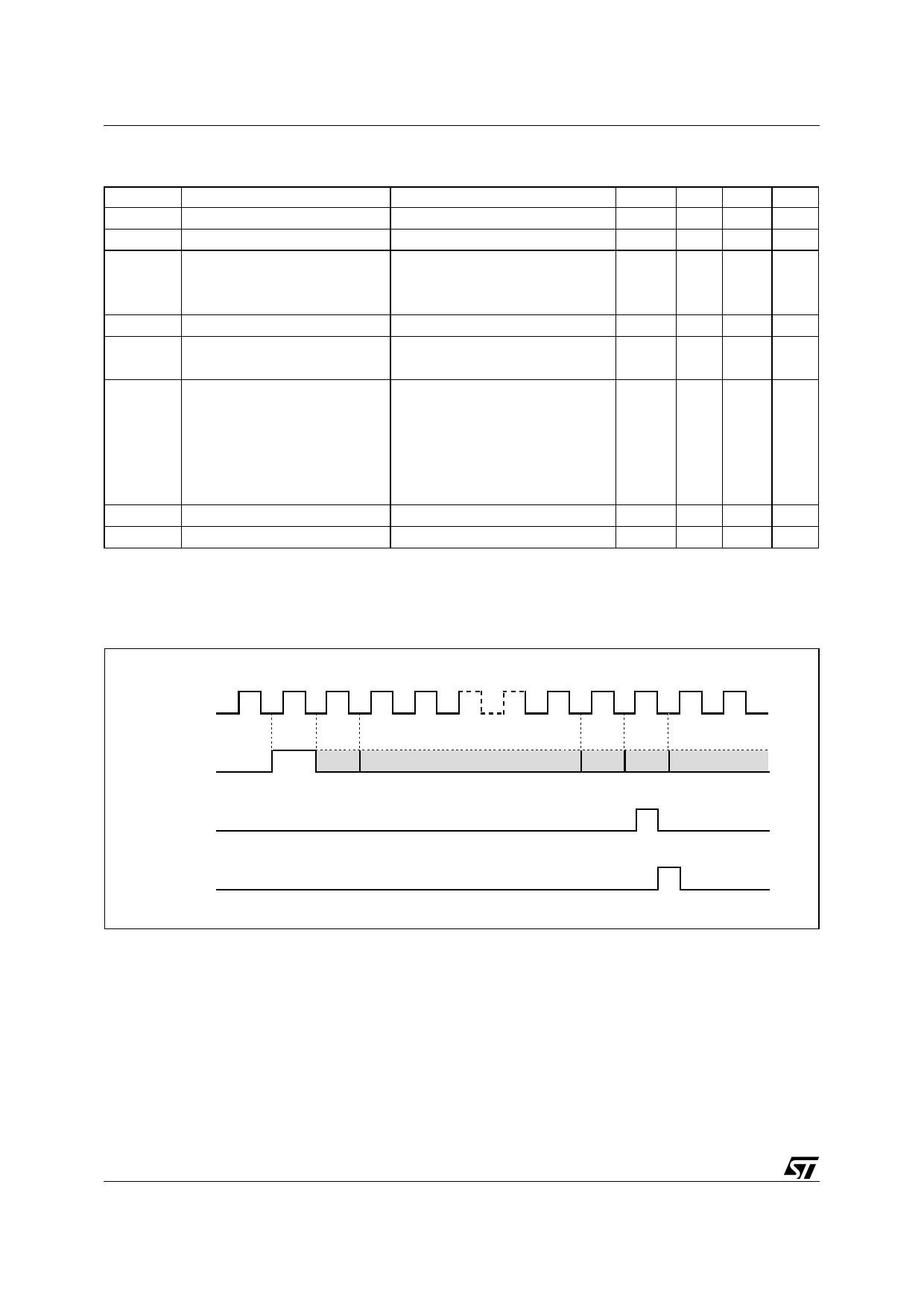
Figure 4. Input Data Format
CLOCK
DATA
1
START BIT 1
36
BIT 34 BIT 35
LOAD
(INTERNAL)
RESET
(INTERNAL)
4/12
Share Link: 