M5M5V416CWG 데이터 시트보기 (PDF) - Mitsumi
부품명
상세내역
제조사
M5M5V416CWG Datasheet PDF : 10 Pages
| |||
2000.11.22 Ver. 1.0
MITSUBISHI LSIs
M5M5V416CWG -70HI
4194304-BIT (262144-WORD BY 16-BIT) CMOS STATIC RAM
FUNCTION
The M5M5V416CWG is organized as 262144-words by
16-bit. These dev ices operate on a single +2.7~3.0V power
supply , and are directly TTL compatible to both input and
output. Its f ully static circuit needs no clocks and no
ref resh, and makes it usef ul.
The operation mode are determined by a combination of
the dev ice control inputs BC1 , BC2 , S1, S2 , W and OE.
Each mode is summarized in the f unction table.
A write operation is executed whenev er the low lev el W
ov erlaps with the low lev el BC1 and/or BC2 and the low
lev el S1 and the high lev el S2. The address(A0~A17) must
be set up bef ore the write cy cle and must be stable during
the entire cycle.
A read operation is executed by s etting W at a high lev el
and OE at a low lev el while BC1 and/or BC2 and S1 and
S2 are in an activ e state(S1=L,S2=H).
When setting BC1 at the high lev el and other pins are in
an activ e stage , upper-by t e are in a selectable mode in
which both reading and writing are enabled, and lower-byte
are in a non-selectable mode. And when setting BC2 at a
high lev el and other pins are in an activ e stage, lower-
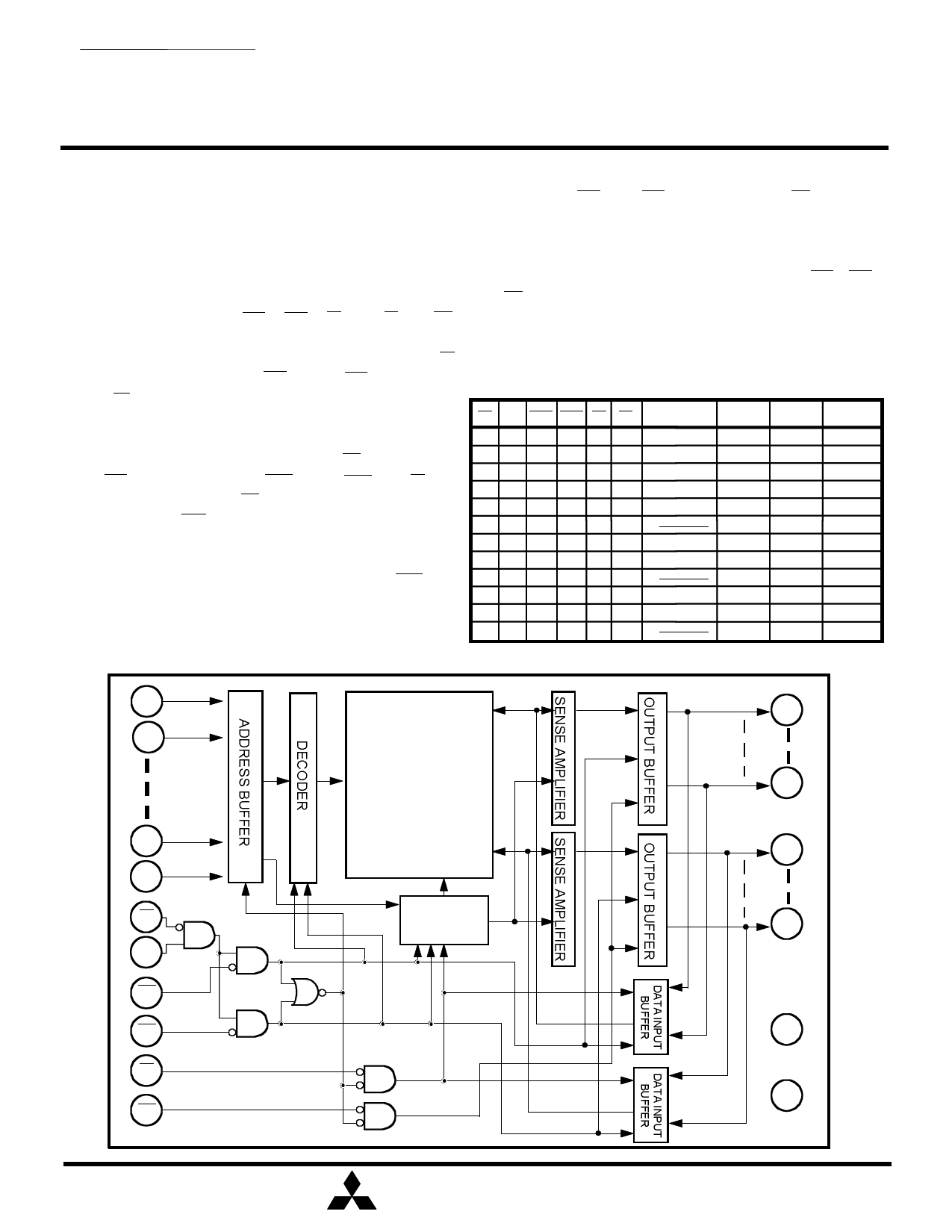
BLOCK DIAGRAM
When setting BC1 and BC2 at a high lev el or S1 at a high
lev el or S2 at a low lev el, the chips are in a non-selectable
mode in which both reading and writing are disabled. In this
mode, the output stage is in a high-impedance state, allowing
OR-tie with other chips and memory expansion by BC1, BC2
and S1, S2.
The power supply c urrent is reduced as low as 0.1µA(25°C,
ty pical), and the memory data can be held at +1V power
supply , enabling battery back-up operation during power
FUNCTION TABLE
S1 S2 BC1 BC2 W OE Mode DQ1~8 DQ9~16 Icc
X L X X X X Non selection High-Z High-Z Standby
H H X X X X Non selection High-Z High-Z Standby
X X H H X X Non selection High-Z High-Z Standby
L H L H L X Write Din High-Z Activ e
L H L H H L Read Dout High-Z Activ e
LH L HH H
High-Z High-Z Activ e
L H H L L X Write High-Z Din Activ e
L H H L H L Read High-Z Dout Activ e
LH H L HH
High-Z High-Z Activ e
L H L L L X Write Din Din Activ e
L H L L H L Read Dout Dout Activ e
LH L L HH
High-Z High-Z Activ e
A0
DQ
1
A1
MEMORY ARRAY
DQ
8
262144 WORDS
x 16 BITS
A16
-
DQ
9
A17
S1
CLOCK
GENERATOR
DQ
16
S2
BC1
BC2
Vcc
W
GND
OE
MITSUBISHI ELECTRIC
2
Share Link: 