M62500P 데이터 시트보기 (PDF) - Mitsumi
부품명
상세내역
제조사
M62500P Datasheet PDF : 11 Pages
| |||
MITSUBISHI (Dig./Ana. INTERFACE)
M62500P/FP
SYNCHRONIZATION DEFLECTION SYSTEM CONTROL PWM IC
SETUP OF VOLTAGE CONTROL BLOCK
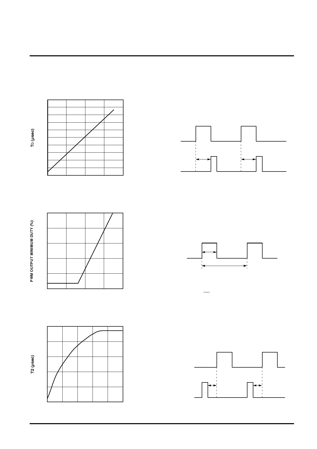
TD vs. VDELAY Adj CHARACTERISTICS (f=40kHz)
20
Applying a voltage to the DELAY Adj pin can control the delay time
of OUT1 to TIN.
10
0
0
2.0
4.0
VDELAY Adj (V)
PWM OUTPUT MINIMUM DUTY vs. VDTC
CHARACTERISTICS (f=40kHz)
100
80
60
40
20
0
0
1
2
3
4
VDTC (V)
TIN
TD
TD
OUT1
Applying a voltage to the DTC pin can control the dead time of
PWM output.
OUT1, 2
TH
T
PWM output minimum duty
TDUTY=
TH
T
X100 (%)
T2 vs. VPhase CHARACTERISTICS (f=40kHz)
10
8
6
4
2
0
0
1
2
3
4
5
VPhase (V)
Applying a voltage to the Phase Adj pin can control a leading time
of drive output to OUT2.
OUT2
T2
T2
DRIVE OUT
( 8 / 11 )
Share Link: 