M7085G(2012) 데이터 시트보기 (PDF) - Unisonic Technologies
부품명
상세내역
제조사
M7085G Datasheet PDF : 7 Pages
| |||
M7085
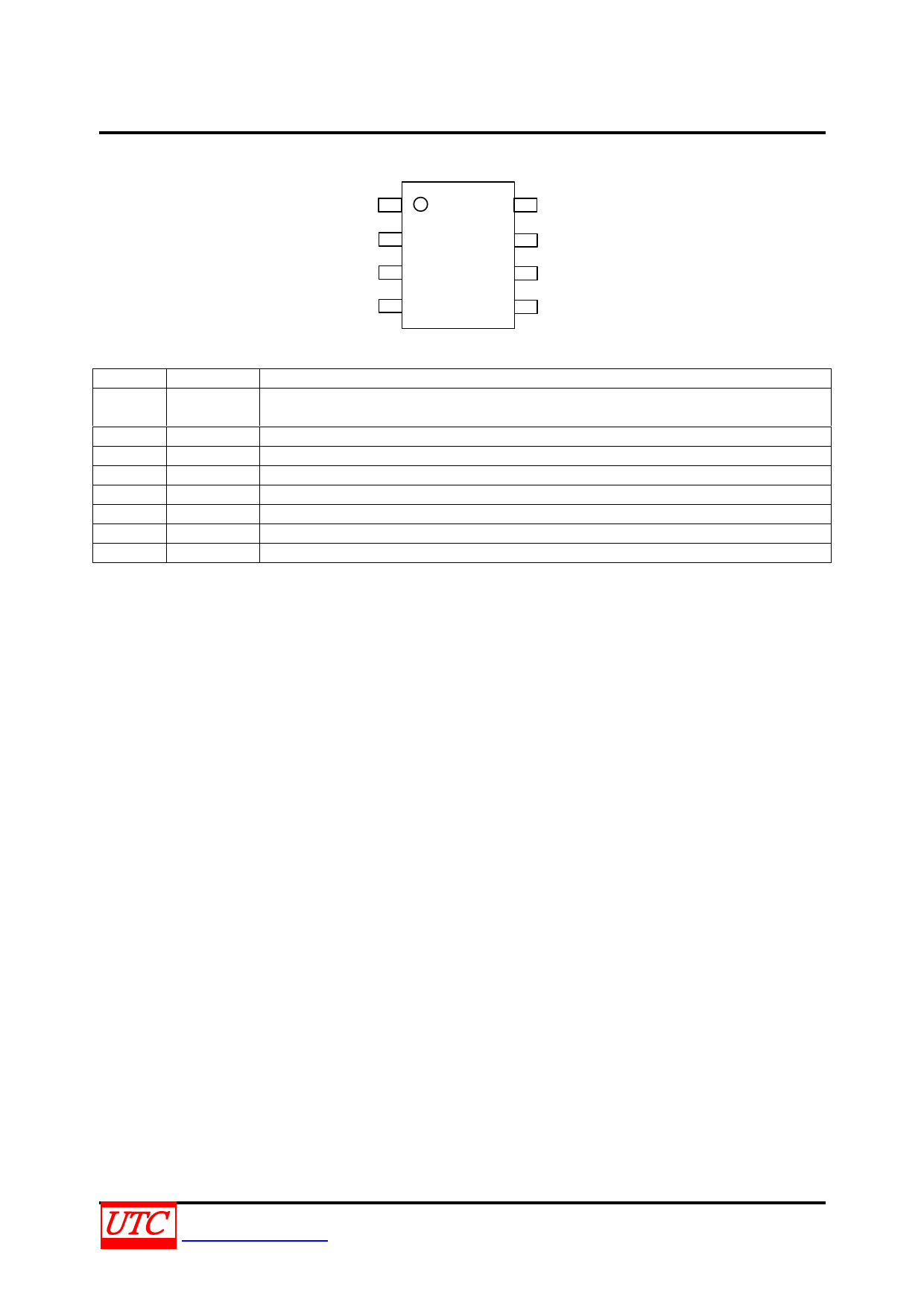
PIN CONFIGURATION
CMOS IC
ISENSE 1
SGND 2
NC 3
FB 4
8 VIN
7 PGATE
6 PGND
5 ADJ
PIN DESCRIPTION
PIN NO
1
2
3
4
5
6
7
8
PIN NAME
ISENSE
SGND
NC
FB
ADJ
PGND
GATE
VIN
DESCRIPTION
The over-current protection input pin that be connected to Drain node of the external
P-Channel.
Signal Ground.
No Connection.
The feedback voltage input.
The over-current protection input pin that adjust current limit threshold.
Power Ground.
Driver pin to Gate of the external P-Channel. PGATE swings between VIN and VIN-5V.
Power Supply
BLOCK DIAGRAM
UNISONIC TECHNOLOGIES CO., LTD
www.unisonic.com.tw
2 of 7
QW-R502-092, Ba
Share Link: 