M80C186XL12 데이터 시트보기 (PDF) - Intel
부품명
상세내역
제조사
M80C186XL12 Datasheet PDF : 44 Pages
| |||
M80C186XL
Symbol
TMR IN 0
TMR IN 1
TMR OUT 0
TMR OUT 1
DRQ0
DRQ1
NMI
INT0
INT1 SELECT
INT2 INTA0
INT3 INTA1 IRQ
A19 S6
A18 S5
A17 S4
A16 S3
AD15
AD14
AD13
AD12
AD11
AD10
AD9
AD8
AD7
AD6
AD5
AD4
AD3
AD2
AD1
AD0
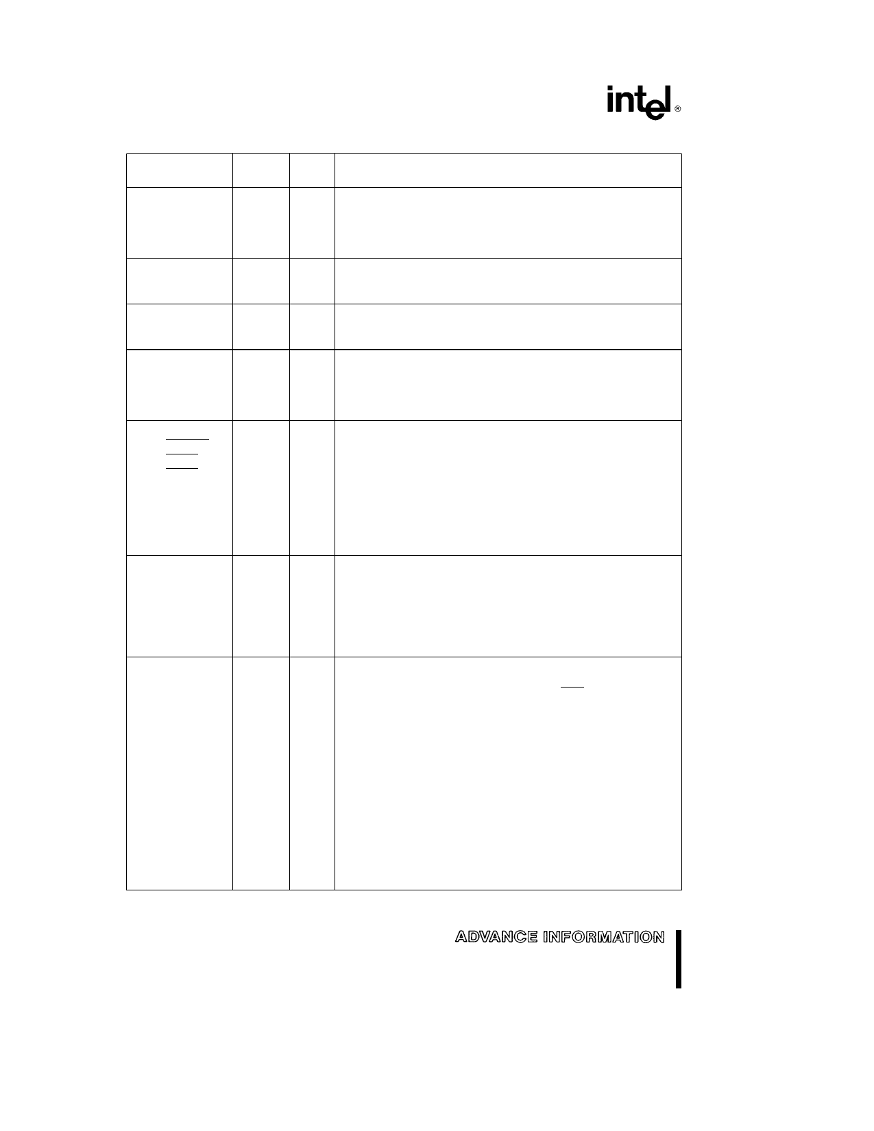
Table 1 M80C186XL Pin Description (Continued)
PGA
Pin No
Type
Name and Function
20
I
Timer Inputs are used either as clock or control signals
21
I
depending upon the programmed timer mode These inputs are
active HIGH (or LOW-to-HIGH transitions are counted) and
internally synchronized Timer Inputs must be tied HIGH when
not being used as clock or retrigger inputs
22
O Timer outputs are used to provide single pulse or continous
23
O waveform generation depending upon the timer mode selected
These outputs are not floated during a bus hold
18
I
DMA Request is asserted HIGH by an external device when it is
19
I
ready for DMA Channel 0 or 1 to perform a transfer These
signals are level-triggered and internally synchronized
46
I
The Non-Maskable Interrupt input causes a Type 2 interrupt An
NMI transition from LOW to HIGH is latched and synchronized
internally and initiates the interrupt at the next instruction
boundary NMI must be asserted for at least one CLKOUT period
The Non-Maskable Interrupt cannot be avoided by programming
45
I
Maskable Interrupt Requests can be requested by activating one
44
I
of these pins When configured as inputs these pins are active
42
I O HIGH Interrupt Requests are synchronized internally INT2 and
41
I O INT3 may be configured to provide active-LOW interrupt-
acknowledge output signals All interrupt inputs may be
configured to be either edge- or level-triggered To ensure
recognition all interrupt requests must remain active until the
interrupt is acknowledged When Slave Mode is selected the
function of these pins changes (see Interrupt Controller section
of this data sheet)
65
O Address Bus Outputs (16 – 19) and Bus Cycle Status (3 – 6)
66
O indicate the four most significant address bits during T1 These
67
O signals are active HIGH
68
O During T2 T3 TW and T4 the S6 pin is LOW to indicate a CPU-
initiated bus cycle or HIGH to indicate a DMA-initiated or refresh
bus cycle During the same T-states S3 S4 and S5 are always
LOW These outputs are floated during bus hold or reset
1
I O Address Data Bus (0 – 15) signals constitute the time multiplexed
3
I O memory or I O address (T1) and data (T2 T3 TW and T4) bus
5
I O The bus is active HIGH A0 is analogous to BHE for the lower
7
I O byte of the data bus pins D7 through D0 It is LOW during T1
10
12
IO
IO
when a byte is to be transferred onto the lower portion of the bus
in memory or I O operations These pins are floated during a bus
hold or reset
14
IO
16
IO
2
IO
4
IO
6
IO
8
IO
11
IO
13
IO
15
IO
17
IO
6
Share Link: 