M95160-RMC6P 데이터 시트보기 (PDF) - STMicroelectronics
부품명
상세내역
제조사
M95160-RMC6P Datasheet PDF : 47 Pages
| |||
M95160 M95160-W M95160-R M95160-DF
Instructions
6.4
Write Status Register (WRSR)
The Write Status Register (WRSR) instruction is used to write new values to the Status
Register. Before it can be accepted, a Write Enable (WREN) instruction must have been
previously executed.
The Write Status Register (WRSR) instruction is entered by driving Chip Select (S) low,
followed by the instruction code, the data byte on Serial Data input (D) and Chip Select (S)
driven high. Chip Select (S) must be driven high after the rising edge of Serial Clock (C) that
latches in the eighth bit of the data byte, and before the next rising edge of Serial Clock (C).
Otherwise, the Write Status Register (WRSR) instruction is not executed.
The instruction sequence is shown in Figure 11.
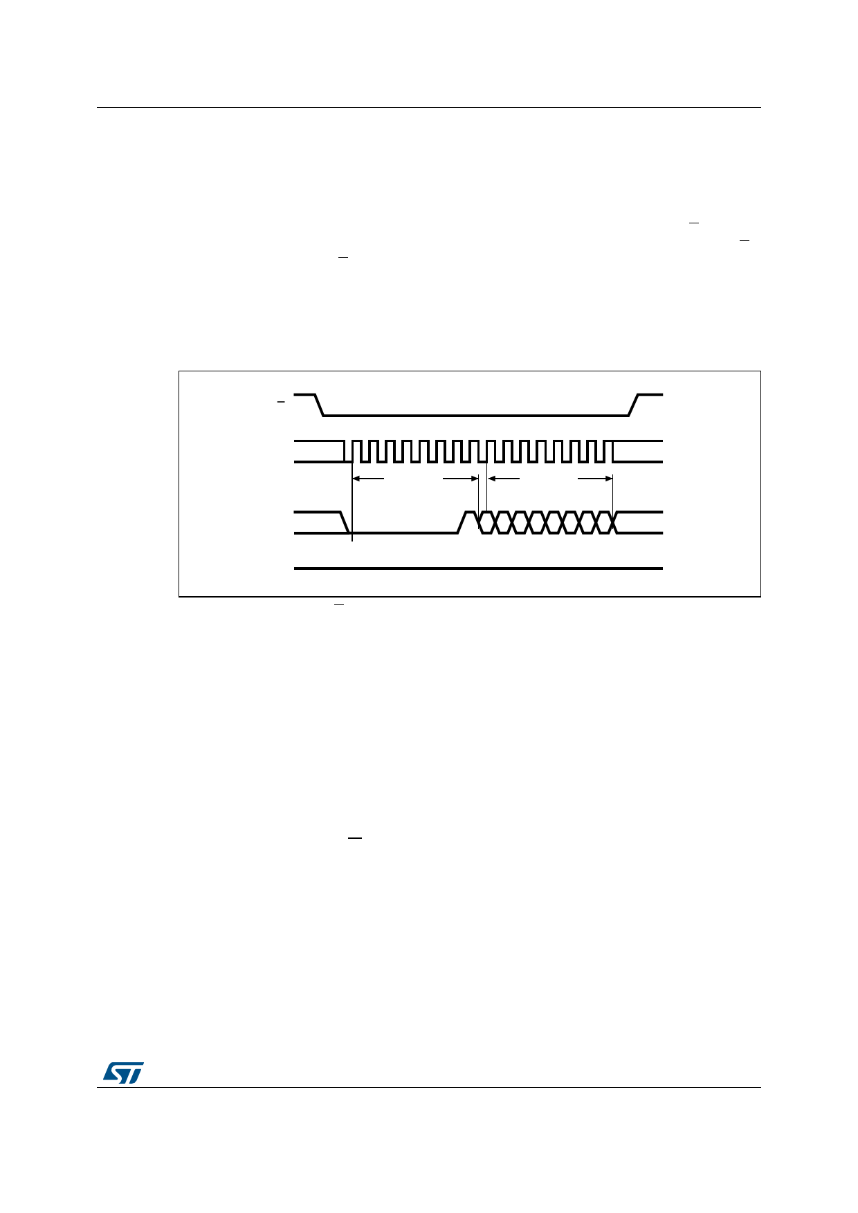
Figure 11. Write Status Register (WRSR) sequence
S
0 1 2 3 4 5 6 7 8 9 10 11 12 13 14 15
C
Instruction
Status
Register In
D
76543210
High Impedance
MSB
Q
AI02282D
Driving the Chip Select (S) signal high at a byte boundary of the input data triggers the self-
timed Write cycle that takes tW to complete (as specified in AC tables under Section 9: DC
and AC parameters).
While the Write Status Register cycle is in progress, the Status Register may still be read to
check the value of the Write in progress (WIP) bit: the WIP bit is 1 during the self-timed
Write cycle tW, and 0 when the Write cycle is complete. The WEL bit (Write Enable Latch) is
also reset at the end of the Write cycle tW.
The Write Status Register (WRSR) instruction enables the user to change the values of the
BP1, BP0 and SRWD bits:
• The Block Protect (BP1, BP0) bits define the size of the area that is to be treated as
read-only, as defined in Table 2.
• The SRWD (Status Register Write Disable) bit, in accordance with the signal read on
the Write Protect pin (W), enables the user to set or reset the Write protection mode of
the Status Register itself, as defined in Table 6. When in Write-protected mode, the
Write Status Register (WRSR) instruction is not executed.
The contents of the SRWD and BP1, BP0 bits are updated after the completion of the
WRSR instruction, including the tW Write cycle.
The Write Status Register (WRSR) instruction has no effect on the b6, b5, b4, b1, b0 bits in
the Status Register. Bits b6, b5, b4 are always read as 0.
DocID022580 Rev 4
21/47
46
Share Link: 