MAX1820 데이터 시트보기 (PDF) - Maxim Integrated
부품명
상세내역
제조사
MAX1820 Datasheet PDF : 18 Pages
| |||
WCDMA Cellular Phone 600mA
Buck Regulators
ELECTRICAL CHARACTERISTICS (continued)
(VBATT = 3.6V, SHDN = BATT, SKIP = SYNC = GND, VREF = 1.25V (MAX1820 only), TA = -40°C to +85°C, unless otherwise noted.)
(Notes 2, 3)
PARAMETER
LX Leakage Current
Maximum Duty Cycle
Minimum Duty Cycle
SYNC AND OSCILLATOR
SYNC Divide Ratio
(MAX1820X)
SYNC Capture Range
(MAX1820X)
SYNC Divide Ratio
(MAX1820Y)
SYNC Capture Range
(MAX1820Y)
SYNC Leakage Current
SYMBOL
CONDITIONS
MIN
ILX
VBATT = 5.5V, LX = GND or BATT
-1
dutyMAX
100
dutyMIN
SKIP = GND
SKIP = BATT, VBATT = 4.2V
SYNC = sine wave, SYNC input = 200mVP-P
13
SYNC = sine wave, SYNC input = 800mVP-P
13
SYNC = sine wave, AC-coupled,
10
SYNC input = 500mVP-P
SYNC = sine wave, SYNC input = 200mVP-P
18
SYNC = sine wave, SYNC input = 800mVP-P
18
SYNC = sine wave, AC-coupled,
15
SYNC input = 500mVP-P
VSYNC = IV (MAX1820Z, MAX1821)
-1
ISYNC
VSYNC = IV (MAX1820X, MAX1820Y, and
-5
MAX1821X)
MAX
1
0
10
UNITS
µA
%
%
13
Hz/Hz
13
16
MHz
18
Hz/Hz
18
21
MHz
+1
µA
+5
Internal Oscillator Frequency
(MAX1820Z, MAX1821)
LOGIC INPUTS (SKIP, SHDN)
Logic Input High
Logic Input Low
Logic Input Current
fOSC
SYNC = GND
VIH
VIL
0.8
1.2
MHz
1.6
V
0.4
V
1
µA
Note 2: Limits are 100% production tested at TA = +25°C for UCSP parts. Limits over the entire operating temperature range are
guaranteed by design and characterization but are not production tested.
Note 3: Specifications to -40°C are guaranteed by design and not subject to production test.
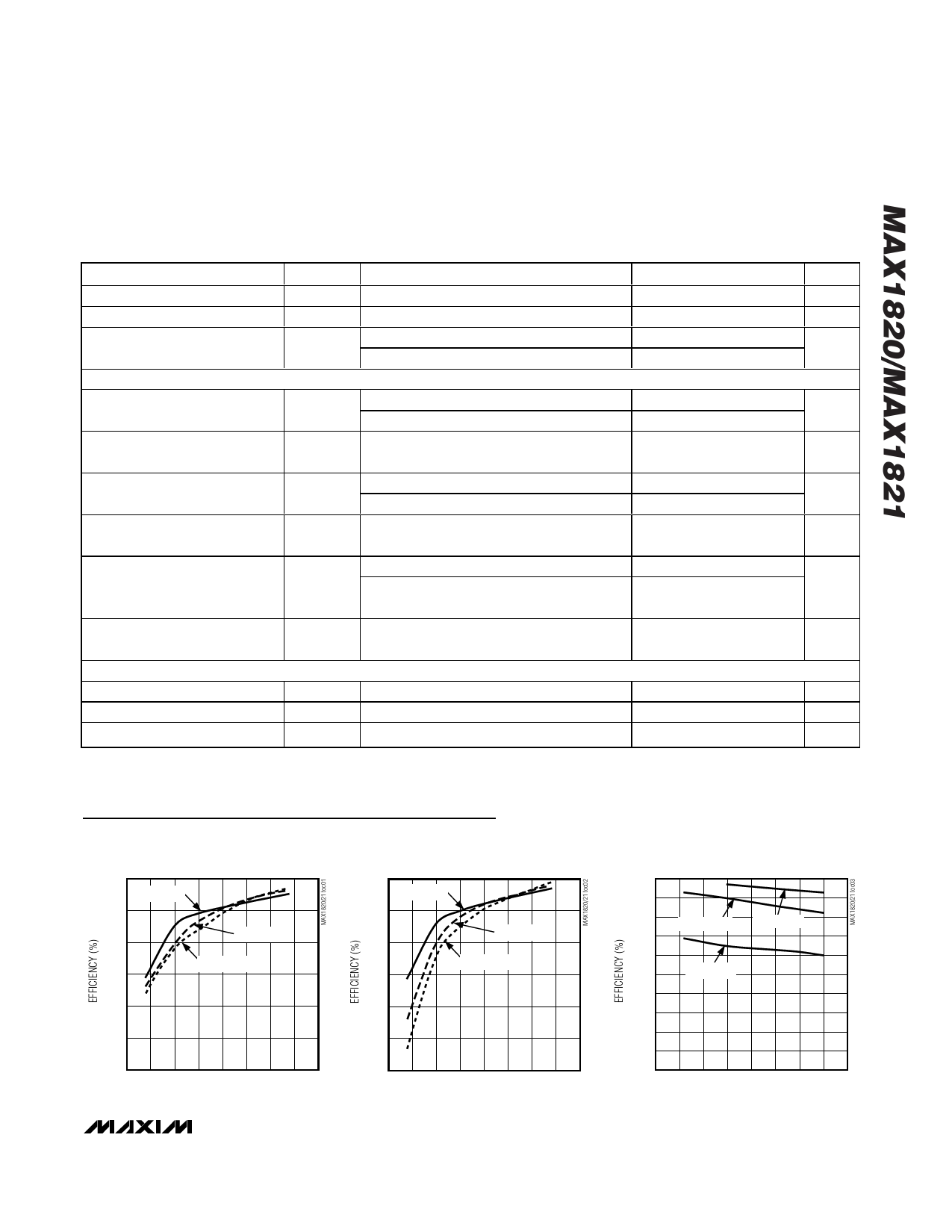
Typical Operating Characteristics
(TA = +25°C, unless otherwise noted.)
EFFICIENCY vs. OUTPUT VOLTAGE
(NORMAL MODE, VIN = 3.6V)
100
RLOAD = 5Ω
90
80
RLOAD = 10Ω
RLOAD = 15Ω
70
EFFICIENCY vs. OUTPUT VOLTAGE
(PWM MODE, VIN = 3.6V)
100
RLOAD = 5Ω
90
RLOAD = 10Ω
80
RLOAD = 15Ω
70
EFFICIENCY vs. INPUT VOLTAGE
NORMAL MODE, RLOAD = 10Ω
100
90
80
VOUT = 1.8V
VOUT = 3.4V
70
60
50
VOUT = 0.4V
40
60
60
30
50
50
20
10
40
0
0.5 1.0 1.5 2.0 2.5 3.0 3.5 4.0
OUTPUT VOLTAGE (V)
40
0
0.5 1.0 1.5 2.0 2.5 3.0 3.5 4.0
OUTPUT VOLTAGE (V)
0
2.0 2.5 3.0 3.5 4.0 4.5 5.0 5.5 6.0
VIN (V)
_______________________________________________________________________________________ 5
Share Link: 