MAX2101 데이터 시트보기 (PDF) - Maxim Integrated
부품명
상세내역
제조사
MAX2101 Datasheet PDF : 24 Pages
| |||
6-Bit Quadrature Digitizer
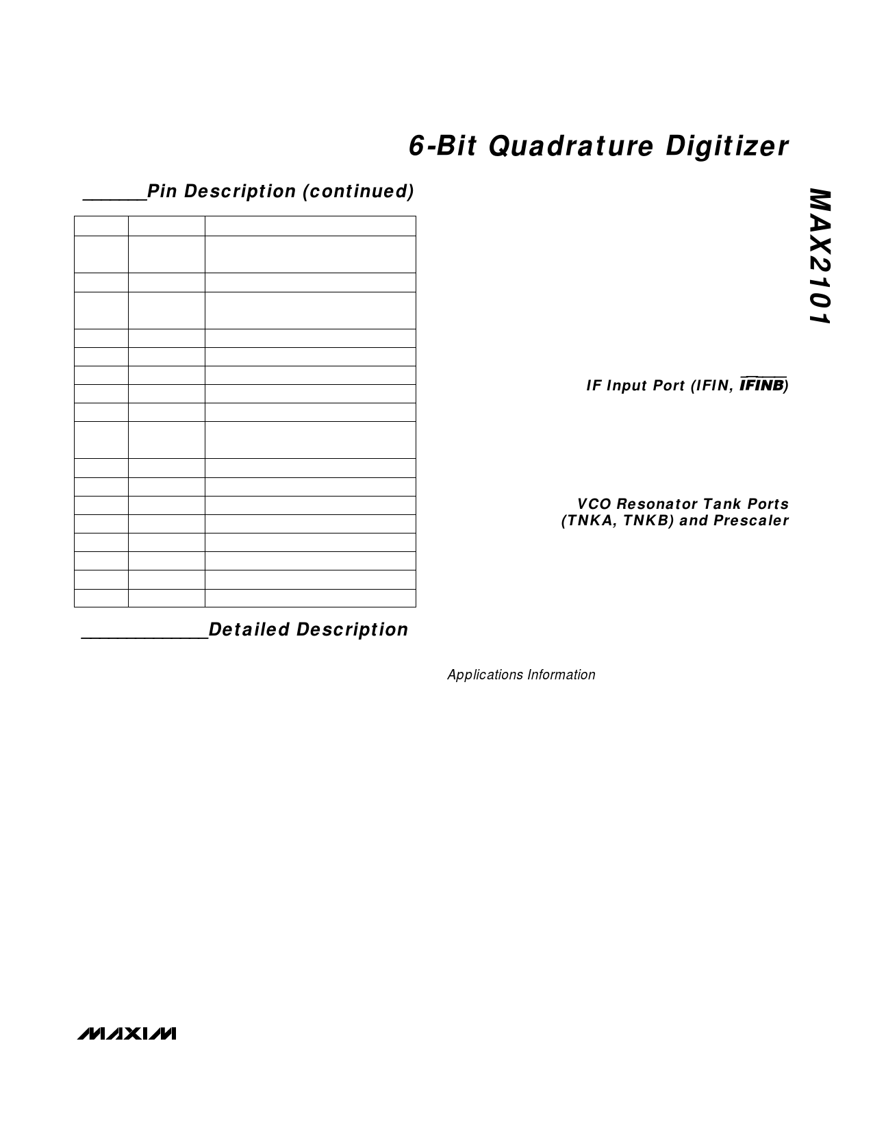
_______Pin Description (continued)
PIN
NAME
FUNCTION
78
BBINI
I Channel Baseband Amplifier,
External Input
79
VGNDI
I Channel Baseband Ground
80
VREFIN
High Impedance, connect to VREF
(pin 88)
81
MIXOUTI I Channel Mixer Output
84
VSUBRF RF Demodulator Substrate
85
PWRI
I Channel Power Indicator
86
2R5
2x VREF Output
87
VCCIF
IF Signal Processing +5V Supply
88
VREF
Bandgap Reference Voltage
Output
90
IFIN
IF Amplifier Noninverting Input
91
IFINB
IF Amplifier Inverting Input
93
AGC
Automatic Gain Control Input
94
VGNDIF IF Signal-Processing Ground
95
FLTRSEL Baseband Signal Path Select
96
PWRQ
Q Channel Power Indicator
97
VPTAT
PTAT Reference Voltage Output
100 MIXOUTQ Q Channel Mixer Output
______________Detailed Description
The MAX2101 6-bit quadrature digitizer solves one of
the most challenging problems of high dynamic range
digital-receiver design by combining quadrature
demodulation and analog-to-digital (A/D) conversion in
a single device. The MAX2101’s unique RF-to-Bits
function bridges the gap between RF downconverters
and CMOS digital signal processors (DSPs). Figure 1
is a simplified connection diagram.
The MAX2101 accepts input signals from 400MHz to
700MHz and applies gain depending on the input
amplitude. The signal is then split and downconverted
to baseband by two mixers, which are driven by two
local oscillator (LO) signals in quadrature. An internal
voltage-controlled oscillator (VCO) feeds the two LOs.
Each baseband is filtered by an internal 5th-order
Butterworth lowpass filter. The on-board lowpass filters
have an externally variable bandwidth of 10MHz to
30MHz. Each baseband is then converted by a 6-bit
analog-to-digital converter (ADC). The conversion result
is stored in a register and is output using the data
clock. See Figure 2 for the relation between baseband
signal, sample and data clock, and digitized data. The
external master clock is internally divided by six and is
available at RCLK for external system functions, fre-
quency synthesizers, etc. See Figures 3 and 4 for func-
tional diagrams.
IF Input Port (IFIN, IFINB)
The MAX2101 provides a balanced IF input. The inputs
are self-biasing, so the input signals should be AC termi-
nated, depending on system requirements. To minimize
noise, the unused input should be AC terminated with
25Ω. To minimize distortion, AC terminate the unused
input with a 50Ω resistor.
VCO Resonator Tank Ports
(TNKA, TNKB) and Prescaler
The MAX2101 integrates a negative impedance oscilla-
tor with balanced inputs. Use a parallel tank network,
as shown in Figure 5. The phase-noise performance of
the oscillator near the carrier is dominated by the reso-
nant network. The resonant inductor must have a suffi-
ciently high Q and a self-resonant frequency (SRF) that
is more than twice the intended LO frequency. Be sure
to minimize parasitic elements surrounding the tank
network by using proper layout techniques. See the
Applications Information section.
The VCO prescaler output provides phase-lock loop
capability for controlling the VCO frequency. The
prescaler generates the VCO frequency divided by 16.
As a result, the prescaler delivers a 25MHz to
43.75MHz signal over the VCO operating frequency
range of 400MHz to 700MHz. The differential outputs
should have equivalent termination.
_______________________________________________________________________________________ 9
Share Link: 