MAX2104(2001) 데이터 시트보기 (PDF) - Maxim Integrated
부품명
상세내역
제조사
MAX2104 Datasheet PDF : 9 Pages
| |||
Direct-Conversion Tuner IC for
Digital DBS Applications
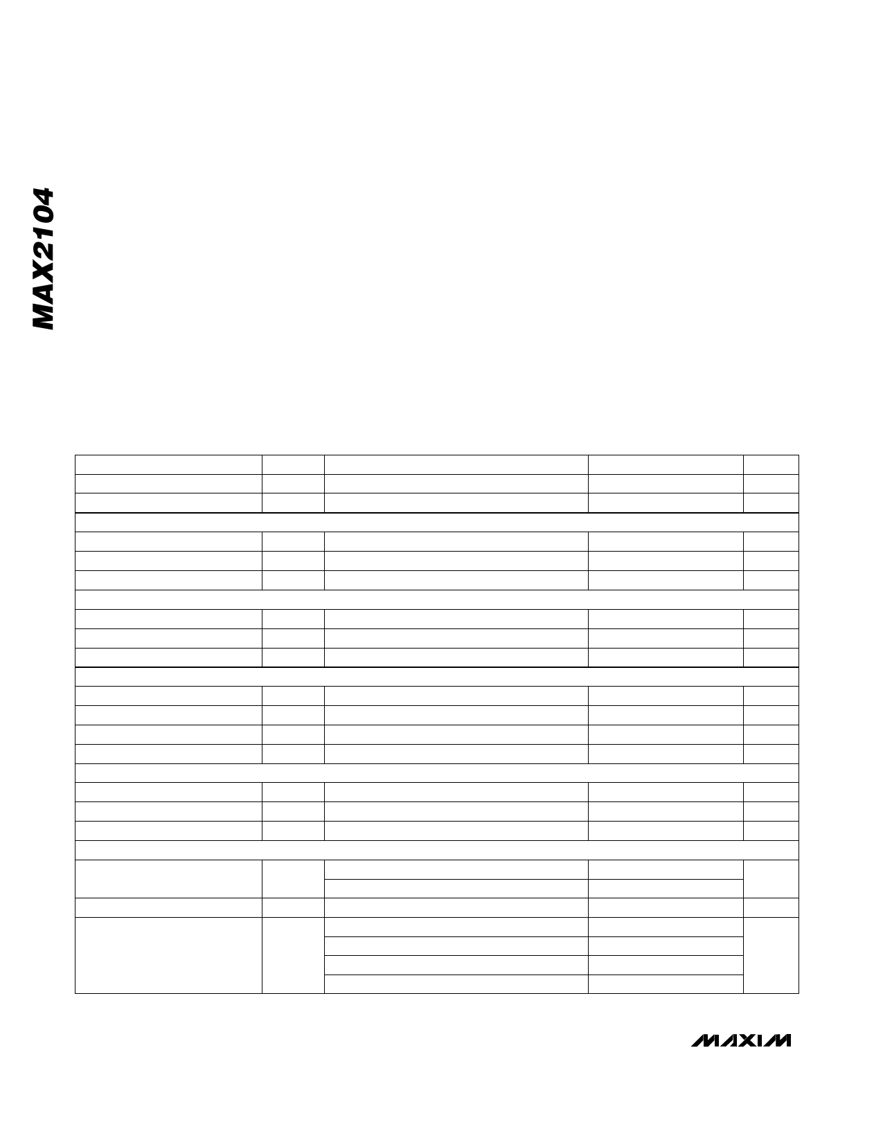
ABSOLUTE MAXIMUM RATINGS
VCC to GND .............................................................-0.5V to +7V
All Other Pins to GND.................................-0.3V to (VCC + 0.3V)
RF1+ to RF1-, RF2+ to RF2-, TANK+ to TANK-,
IDC+ to IDC-, QDC+ to QDC- ............................................±2V
IOUT_, QOUT_ to GND Short-Circuit Duration ......................10s
PSOUT+, PSOUT- to GND Short-Circuit Duration .................10s
Continuous Current (any pin)..............................................20mA
Continuous Power Dissipation (TA = +70°C)
(derate 27mW/°C above +70°C) .......................................1.5W
Operating Temperature Range...............................0°C to +85°C
Junction Temperature ......................................................+150°C
Storage Temperature Range ............................-65°C to +150°C
Lead Temperature (soldering, 10s) ................................+300°C
Stresses beyond those listed under “Absolute Maximum Ratings” may cause permanent damage to the device. These are stress ratings only, and functional
operation of the device at these or any other conditions beyond those indicated in the operational sections of the specifications is not implied. Exposure to
absolute maximum rating conditions for extended periods may affect device reliability.
DC ELECTRICAL CHARACTERISTICS
(VCC = 4.75V to 5.25V, VFB = 2.4V, CIOUT_ = CQOUT_ = 10pF, fFLCLK = 2MHz, RFIN_ = floating, RIOUT_ = RQOUT_ = 10kΩ,
VFDOUB = VINSEL = VCPG1 = VCPG2 = 2.4V, VPLLIN+ = VMOD+ = 1.3V, VPLLIN- = VMOD- = 1.1V, TA = +25°C. Typical values are at
VCC = 5.0V and TA = +25°C, unless otherwise noted.)
PARAMETER
SYMBOL
CONDITIONS
MIN TYP MAX UNITS
Operating Supply Voltage
VCC
Operating Supply Current
ICC
STANDARD DIGITAL INPUTS (FDOUB, INSEL, CPG1, CPG2)
4.75
5.25
V
190
275
mA
Digital Input Voltage High
VIH
Digital Input Voltage Low
VIL
Digital Input Current
IIN
SLEW-RATE-LIMITED DIGITAL INPUTS
2.4
V
0.5
V
-15
+10
µA
FLCLK Input Voltage High
1.85
V
FLCLK Input Voltage Low
1.45
V
FLCLK Input Current (Note 1)
RSOURCE = 50kΩ, VFLCLK = 1.65V
DIFFERENTIAL DIGITAL INPUTS (MOD+, MOD-, PLLIN+, PLLIN-)
-1
+1
µA
Common-Mode Input Voltage
Input Voltage Low (Note 2)
Input Voltage High (Note 2)
Input Current (Note 1)
VCMI
Referenced to VCMI
Referenced to VCMI
1.08
1.2
1.32
V
-100 mV
100
mV
-5
5
µA
DIFFERENTIAL DIGITAL OUTPUTS (PSOUT+, PSOUT-)
Common-Mode Output Voltage
Output Voltage Low (Note 3)
Output Voltage High (Note 3)
FREQUENCY SYNTHESIZER
VCMO
Referenced to VCMO
Referenced to VCMO
2.16
2.4
2.64
V
-215 -150 mV
150
215
mV
Prescaler Ratio
Reference Divider Ratio
(VMOD+ - VMOD-) = 200mV
(VMOD+ - VMOD-) = -200mV
32
32
33
33
8
8
Charge-Pump Output High
Measured at FB
VCPG1 = VCPG2 = 0.5V
VCPG1 = 0.5V, VCPG2 = 2.4V
VCPG1 = 2.4V, VCPG2 = 0.5V
VCPG1 = VCPG2 = 2.4V
0.08
0.1
0.12
0.24
0.3
0.36
mA
0.48
0.6
0.72
1.44
1.8
2.16
2 _______________________________________________________________________________________
Share Link: 