LC75811E 데이터 시트보기 (PDF) - SANYO -> Panasonic
부품명
상세내역
제조사
LC75811E Datasheet PDF : 27 Pages
| |||
LC75811E, 75811W
Reset Function
The LC75811E and LC75811W are reset when a low level is applied to the RES pin at power on and, in normal mode.
On a reset the LC75811E and LC75811W create a display with all LCD panels turned off. However, after a reset
applications must set the contents of DCRAM, ADRAM, and CGRAM before turning on display with a “display on/off
control” instruction since the contents of these memories are undefined. That is, applications must execute the following
instructions.
• Set display technique
• DCRAM data write
• ADRAM data write (If ADRAM is used.)
• CGRAM data write (If CGRAM is used.)
• Set AC address
After executing the above instructions, applications must turn on the display with a “display on/off control” instruction.
Note that when applications turn off in the normal mode, applications must turn off the display with a “display on/off
control” instruction. (See the detailed instruction descriptions.)
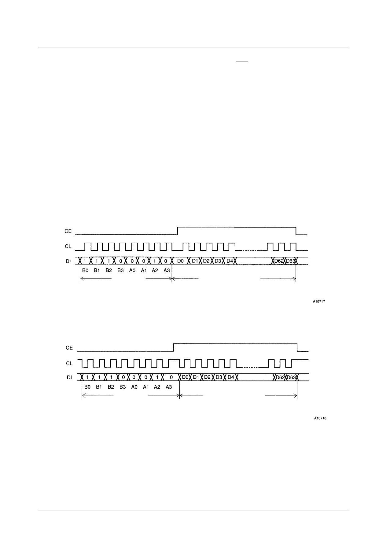
Serial Data Transfer Format
• When CL is stopped at the low level
CCB address
8 bits
• When CL is stopped at the high level
Instruction data
Up to 64 bits
CCB address
8 bits
Instruction data
Up to 64 bits
• CCB address: 47H
• D0 to D63: Instruction data
The data is acquired on the rising edge of the CL signal and latched on the falling edge of the CE signal. When
transferring instruction data from the microcontroller, applications must assure that the time from the transfer of one set
of instruction data until the next instruction data transfer is significantly longer than the instruction execution time.
No. 5915-9/27
Share Link: 