MAX2830 데이터 시트보기 (PDF) - Maxim Integrated
부품명
상세내역
제조사
MAX2830
Maxim Integrated

MAX2830 Datasheet PDF : 33 Pages
| |||
2.4GHz to 2.5GHz 802.11g/b RF Transceiver, PA,
and Rx/Tx/Antenna Diversity Switch
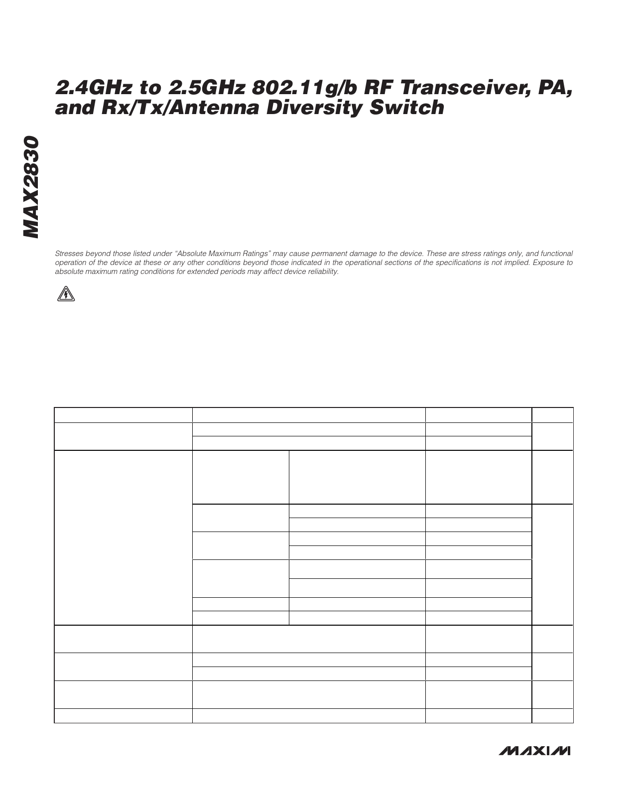
ABSOLUTE MAXIMUM RATINGS
VCCTXPA, VCCPA, and ANT_ _ to GND ..................-0.3V to +4.5V
VCCLNA, VCCTXMX, VCCPLL, VCCCP, VCCXTAL, VCCVCO,
VCCRXVGA, VCCRXFL, and VCCRXMX_ to GND...-0.3V to +3.9V
B6, B7, B3, B2, SHDN, B5, CS, SCLK, DIN, B1, TUNE, B4,
ANTSEL, TXBBI_, TXBBQ_, RXHP, RXTX, RXBBI_, RXBBQ_,
RSSI, BYPASS, CPOUT, LD, CLOCKOUT, XTAL,
CTUNE to GND ....................-0.3V to (Operating VCC + 0.3V)
RXBBI_, RXBBQ_, RSSI, BYPASS, CPOUT, LD, CLOCKOUT
Short-Circuit Duration .........................................................10s
RF Input Power ...............................................................+10dBm
Continuous Power Dissipation (TA = +70°C)
48-Pin TQFN (derates 27.8mW/°C above +70°C) .........2.22W
Operating Temperature Range ...........................-40°C to +85°C
Junction Temperature ......................................................+150°C
Storage Temperature Range .............................-65°C to +160°C
Lead Temperature (soldering, 10s) .................................+300°C
Soldering Temperature (reflow) .......................................+260°C
Stresses beyond those listed under “Absolute Maximum Ratings” may cause permanent damage to the device. These are stress ratings only, and functional
operation of the device at these or any other conditions beyond those indicated in the operational sections of the specifications is not implied. Exposure to
absolute maximum rating conditions for extended periods may affect device reliability.
CAUTION! ESD SENSITIVE DEVICE
DC ELECTRICAL CHARACTERISTICS
(MAX2830 EV kit, VCC_ = 2.7V to 3.6V, VCCPA = VCCTXPA = 2.7V to 4.2V, TA = -40°C to +85°C, Rx set to the maximum gain. CS =
high, RXHP = SCLK = DIN = ANTSEL = low, RSSI and clock output buffer are off, no signal at RF inputs, all RF inputs and outputs
terminated into 50Ω, receiver baseband outputs are open. 100mVRMS differential I and Q signals (54Mbps IEEE 802.11g OFDM)
applied to I/Q baseband inputs of transmitter in transmit mode, fREF = 40MHz, and registers set to recommended settings and corre-
sponding test mode, unless otherwise noted. Typical values are at VCC = 2.8V, VCCPA = 3.3V, and TA = +25°C, LO frequency =
2.437GHz, unless otherwise noted. RF inputs/outputs specifications are referenced to device pins and do not include 1dB loss from
EV kit PCB, balun, and SMA connectors.) (Note 1)
PARAMETERS
Supply Voltage
VCC_
VCCPA, VCCTXPA
CONDITIONS
Shutdown mode,
B7: B1 = 0000000,
reference oscillator not
applied
TA = +25°C
MIN TYP MAX UNITS
2.7
3.6
V
2.7
4.2
20
µA
Supply Current
Rx I/Q Output Common-Mode
Voltage
Rx I/Q Output Common-Mode
Voltage Variation
Tx Baseband Input Common-
Mode Voltage Operating Range
Tx Baseband Input Bias Current
Standby mode
Rx mode
Tx mode, TA = +25°C,
VCC = 2.8V, VCCPA =
3.3V (Note 2)
Rx calibration mode
Tx calibration mode
TA = +25°C
TA = -40°C to +85°C
TA = +25°C
TA = -40°C to +85°C
Transmit section
PA, POUT = +17.1dBm
TA = +25°C
TA = +25°C
TA = +25°C at default common-mode setting
TA = -40°C (relative to TA = +25°C)
TA = +85°C (relative to TA = +25°C)
DC-coupled
Source current
28
35
35
62
78
82
82
104
mA
212
101
78
0.94 1.2 1.37
V
-17
mV
15
0.9
1.3
V
22
µA
2 _______________________________________________________________________________________
Share Link: