MAX4528 데이터 시트보기 (PDF) - Maxim Integrated
부품명
상세내역
제조사
MAX4528 Datasheet PDF : 12 Pages
| |||
Low-Voltage, Phase-Reversal
Analog Switch
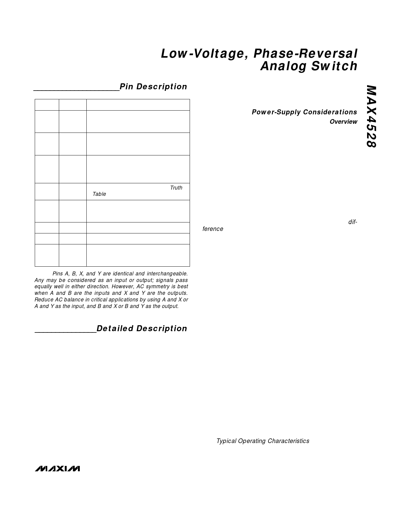
_____________________Pin Description
PIN NAME
FUNCTION
Analog-Switch Input Terminal A.
1
A
Connected to Y when IN is low; con-
nected to X when IN is high.
Analog-Switch Input Terminal B.
2
B
Connected to X when IN is low; con-
nected to Y when IN is high.
Ground. Connect GND to digital
3
GND
ground. (Analog signals have no
ground reference; they are limited to
V+ and V-.)
4
IN
Logic-Level Control Inputs (see Truth
Table)
Negative Analog Supply-Voltage
5
V-
Input. Connect V- to GND for single-
supply operation.
6
Y
Analog-Switch Output Terminal Y
7
X
Analog-Switch Output Terminal X
Positive Analog/Digital Supply-Voltage
8
V+
Input. Internally connected to sub-
strate.
Note: Pins A, B, X, and Y are identical and interchangeable.
Any may be considered as an input or output; signals pass
equally well in either direction. However, AC symmetry is best
when A and B are the inputs and X and Y are the outputs.
Reduce AC balance in critical applications by using A and X or
A and Y as the input, and B and X or B and Y as the output.
_______________Detailed Description
The MAX4528 is a phase-reversal analog switch consist-
ing of two normally open and two normally closed CMOS
analog switches arranged in a bridge configuration.
Analog signals are put into two input pins and taken out
of two output pins. A logic-level signal controls whether
the input signal is routed through normally or inverted. A
low-resistance DC path goes from inputs to outputs at all
times, yet isolation between the two signal paths is excel-
lent. Analog signals range from V- to V+.
These parts are characterized and optimized with ±5V
supplies, and can operate from a single supply.
The MAX4528 is designed for DC and low-frequency-
signal phase-reversal applications, such as chopper
amplifiers, modulator/demodulators, and self-zeroing or
self-calibrating circuits. Unlike conventional CMOS
switches externally wired in a bridge configuration,
both DC and AC symmetry are optimized with a small
8-pin configuration that allows simple board layout and
isolation of logic signals from analog signals.
Power-Supply Considerations
Overview
The MAX4528’s construction is typical of most CMOS
analog switches. It has three supply pins: V+, V-, and
GND. V+ and V- drive the internal CMOS switches and
set the analog-voltage limits on any switch. Reverse
ESD-protection diodes are internally connected
between each analog-signal pin and both V+ and V-.
One of these diodes conducts if any analog signal
exceeds V+ or V-.
Virtually all of the analog leakage current is through the
ESD diodes to V+ or V-. Although the ESD diodes on a
given signal pin are identical and therefore fairly well
balanced, they are reverse biased differently. Each is
biased by either V+ or V- and the analog signal. This
means their leakages vary as the signal varies. The dif-
ference in the two diode leakages from the signal path
to the V+ and V- pins constitutes the analog-signal-path
leakage current. All analog leakage current flows to the
supply terminals, not to the other switch terminal. This
explains how both sides of a given switch can show
leakage currents of either the same or opposite polarity.
There is no connection between the analog-signal
paths and GND. The analog-signal paths consist of an
N-channel and P-channel MOSFET with their sources
and drains paralleled and their gates driven out-of-
phase to V+ and V- by the logic-level translators.
V+ and GND power the internal logic and logic-level
translator and set the input logic threshold. The logic-
level translator converts the logic levels to switched V+
and V- signals to drive the analog switches’ gates. This
drive signal is the only connection between GND and
the analog supplies. V+ and V- have ESD-protection
diodes to GND. The logic-level input has ESD protec-
tion to V+ and V-, but not to GND, so the logic signal
can go below GND (as low as V-) when bipolar sup-
plies are used.
Increasing V- has no effect on the logic-level thresholds,
but it does increase the drive to the internal P-channel
switches, reducing overall switch on-resistance. V- also
sets the negative limit of the analog-signal voltage.
The logic-level input pin (IN) has ESD-protection diodes
to V+ and V- but not to GND, so it can be safely driven
to V+ and V-. The logic-level threshold (VIN) is CMOS/
TTL compatible when V+ is between 4.5V and 12V
(see Typical Operating Characteristics).
_______________________________________________________________________________________ 7
Share Link: 