MAX4528 데이터 시트보기 (PDF) - Maxim Integrated
부품명
상세내역
제조사
MAX4528 Datasheet PDF : 12 Pages
| |||
Low-Voltage, Phase-Reversal
Analog Switch
Bipolar Supplies
The MAX4528 operates with bipolar supplies between
±2.7V and ±6.0V. The V+ and V- supplies need not be
symmetrical, but their sum cannot exceed the 13V
absolute maximum rating (see Absolute Maximum
Ratings).
Single Supply
The MAX4528 operates from a single +2.7V to +12V
supply when V- is connected to GND. Observe all of
the bipolar precautions when operating from a single
supply.
__________Applications Information
The MAX4528 is designed for DC and low-frequency-
signal phase-reversal applications. Both DC and AC
symmetry are optimized for use with ±5V supplies.
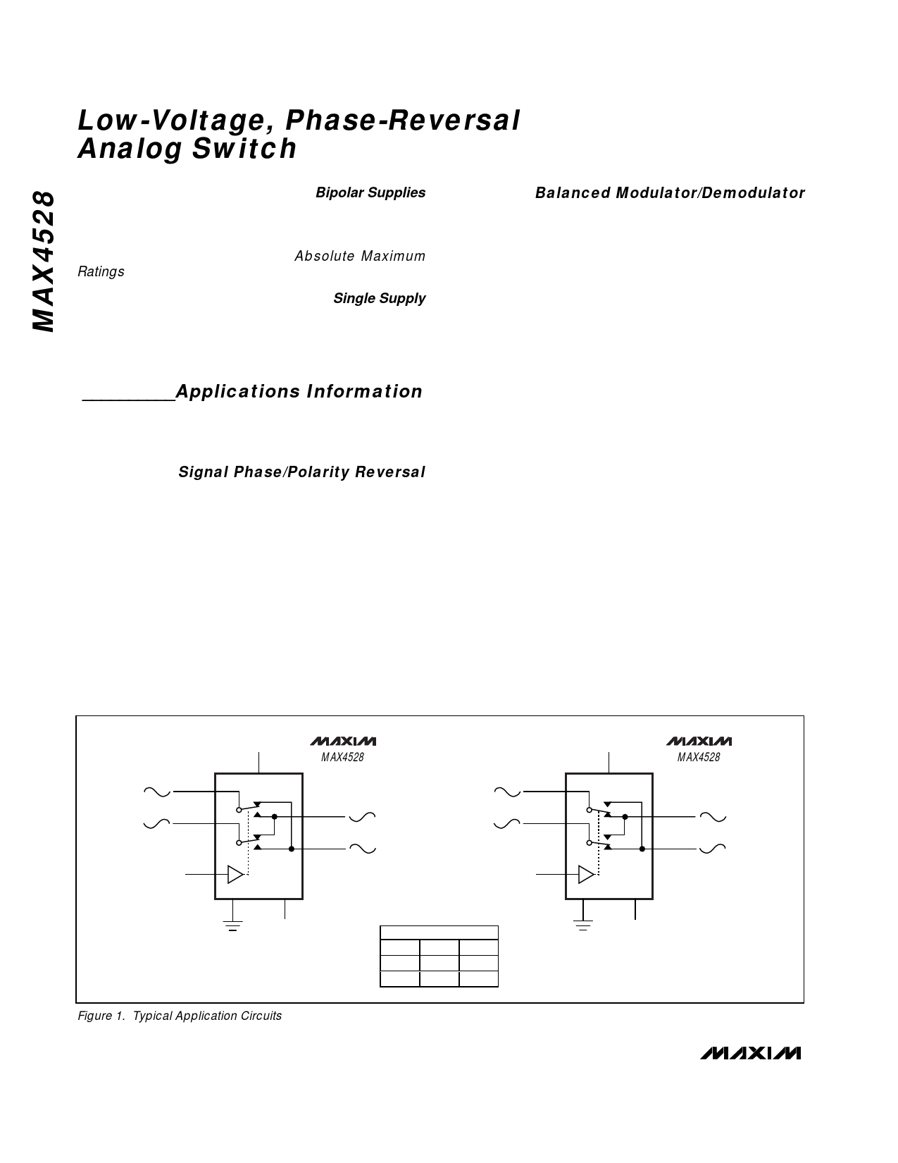
Signal Phase/Polarity Reversal
The MAX4528 can reverse the phase or polarity of a
pair of signals that are out-of-phase and balanced to
ground. This is done by routing signals through the
MAX4528 and, under control of IN, reversing the two
signals paths inside the switch before sending out to a
balanced output. Figure 1 shows a typical example.
The MAX4528 cannot reverse the phase or polarity
of a single grounded signal, as can be done with an
inverting op amp or transformer.
Balanced Modulator/Demodulator
The MAX4528 can be used as a balanced modulator/
demodulator at carrier frequencies up to 100kHz
(Figure 2). Higher frequencies are possible, but as fre-
quency increases, small imbalances in the MAX4528’s
internal capacitance and resistance gradually impair
performance. Similarly, imbalances in external circuit
capacitance and resistance to GND reduce overall car-
rier suppression.
The carrier is applied as a logic-level square wave to
IN. (Note that this voltage can go as negative as V-.)
For best carrier suppression, the power-supply volt-
ages should be equal, the square wave should have a
precise 50% duty cycle, and both the input and output
signals should be symmetrical around ground. Bypass
V+ and V- to GND with 0.1µF ceramic capacitors, as
close to the IC pins as possible. In critical applications,
carrier suppression can be optimized by trimming duty
cycle, DC bias around GND, or external source and
load capacitance.
In signal lines, balancing both capacitance and resis-
tance to GND produces the best carrier suppression.
Transformer coupling of input and output signals
provides the best isolation and carrier suppression.
Transformers can also provide signal filtering, imped-
ance matching, or low-noise voltage gain. Use a
center-tapped transformer or high-resistance voltage
divider to provide a DC path to GND on either the input
or output signal. This ensures a DC path to GND and
symmetrical operation of the internal switches.
INPUTS
LOGIC LOW
V+
A
V+
B
X
Y
IN
GND
V-
MAX4528
OUTPUTS
INPUTS
LOGIC HIGH
V+
A
V+
B
X
Y
IN
GND
V-
MAX4528
OUTPUTS
V-
TRUTH TABLE
V-
IN
A
B
O
Y
X
1
X
Y
Figure 1. Typical Application Circuits
8 _______________________________________________________________________________________
Share Link: 