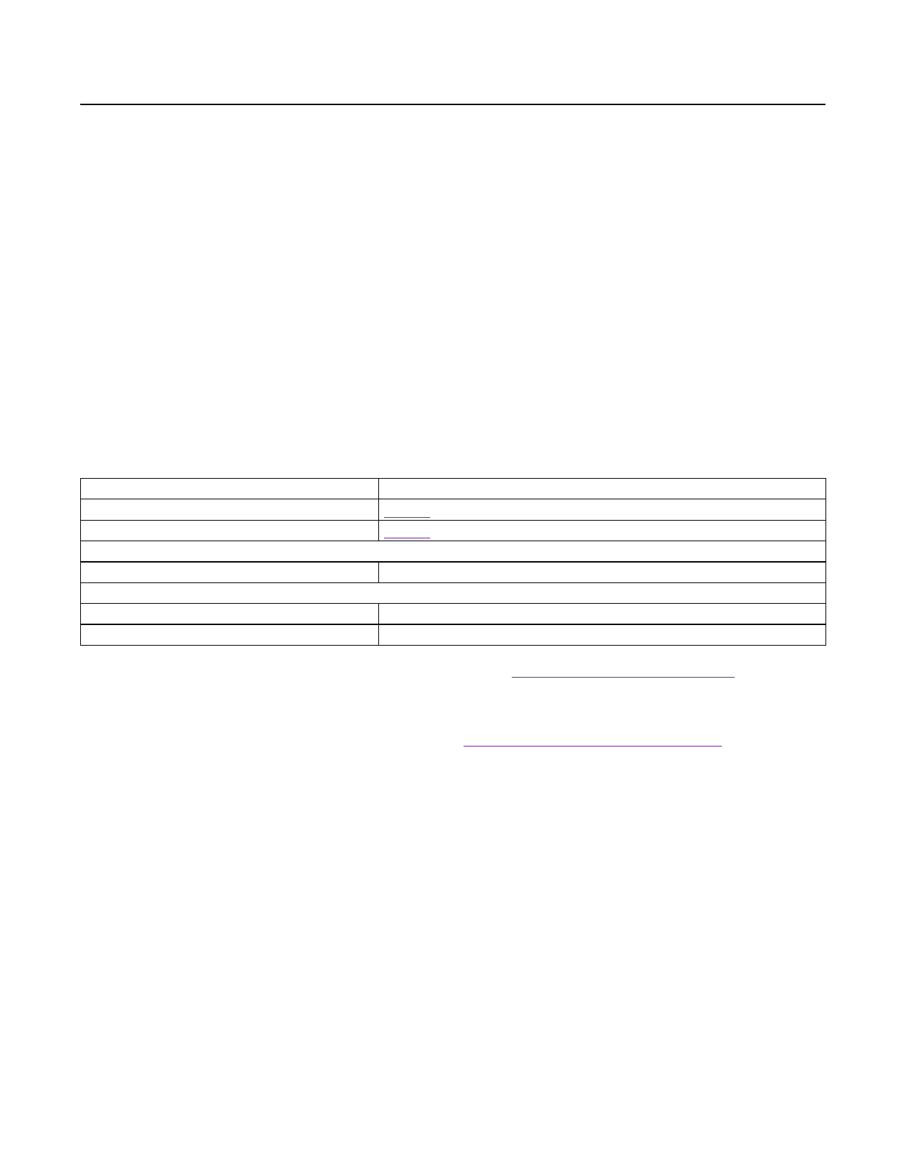
MAX6323(2003) 데이터 시트보기 (PDF) - Maxim Integrated
부품명
상세내역
제조사
MAX6323
(Rev.:2003)
(Rev.:2003)
Maxim Integrated

MAX6323 Datasheet PDF : 12 Pages
| |||
µP Supervisory Circuits with Windowed
(Min/Max) Watchdog and Manual Reset
ABSOLUTE MAXIMUM RATINGS
Terminal Voltage (with respect to GND)
VCC ..................................................................-0.3V to +6.0V
MR, RESET (MAX6323), WDI .............-0.3V to (VCC + +0.3V)
WDPO, RESET (MAX6324) ..............................-0.3V to +6.0V
Input Current, VCC, WDI, MR ..............................................20mA
Output Current, RESET, WDPO ..........................................20mA
Rate of Rise, VCC ............................................................100V/µs
Continuous Power Dissipation (TA = +70°C)
6-Pin SOT23 (derate 8.7mW/°C above +70°C) ..........696mW
Operating Temperature Range .........................-40°C to +125°C
Junction Temperature ......................................................+150°C
Storage Temperature Range .............................-65°C to +150°C
Lead Temperature (soldering, 10s) .................................+300°C
Stresses beyond those listed under “Absolute Maximum Ratings” may cause permanent damage to the device. These are stress ratings only, and functional
operation of the device at these or any other conditions beyond those indicated in the operational sections of the specifications is not implied. Exposure to
absolute maximum rating conditions for extended periods may affect device reliability.
ELECTRICAL CHARACTERISTICS
(VCC = full range, TA = -40°C to +125°C, unless otherwise noted. Typical values are at VCC = 3V, TA = +25°C.) (Note 1)
PARAMETER
SYMBOL
CONDITIONS
MIN TYP MAX
Operating Voltage Range
Supply Current
VCC
ICC
No load, RESET
deasserted
MAX632_ _UT46
VCC = 2.5V or 3.3V
VCC = 5.5V
1.2
5.5
23
45
27
57
4.50 4.63 4.75
MAX632_ _UT44
4.25 4.38 4.50
Reset Threshold Voltage
MAX632_ _UT31
VTH
MAX632_ _UT29
3.00 3.08 3.15
2.85 2.93 3.00
MAX632_ _UT26
2.55 2.63 2.70
Reset Timeout Delay
VCC to RESET Delay
WDPO, RESET Output Voltage
MAX632_ _UT23
2.25 2.32 2.38
tRP
RESET deasserted
100
180
280
10mV/ms, VTH +100mV to VTH -100mV
20
ISINK = 1.2mA, VCC = 2.25V (MAX632_ _UT23,
MAX632_ _UT26, MAX632_ _UT29,
0.4
MAX632_ _UT31)
VOL
ISINK = 3.2mA, VCC = 4.25V (MAX632_ _UT44,
MAX632_ _UT46)
0.4
RESET Output Voltage
(MAX6323)
ISINK = 100µA, VCC > 1.2V, RESET asserted
0.4
ISOURCE = 500µA, VCC = 3.15V, RESET
deasserted (MAX632_ _UT23, MAX632_ _UT26, 0.8 x VCC
VOH MAX632_ _UT29, MAX632_ _UT31)
ISOURCE = 800µA, VCC = 4.75V, RESET
deasserted, (MAX632_ _UT44, MAX632_ _UT46)
VCC - 1.5
WDPO, RESET Output Leakage
ILKG
V RESET = V WDPO = +5.5V, RESET, WDPO
deasserted
1
UNITS
V
µA
V
ms
µs
V
V
µA
2 _______________________________________________________________________________________
Share Link: