MAX6951EEE 데이터 시트보기 (PDF) - Maxim Integrated
부품명
상세내역
제조사
MAX6951EEE Datasheet PDF : 19 Pages
| |||
Serially Interfaced, +2.7V to +5.5V,
5- and 8-Digit LED Display Drivers
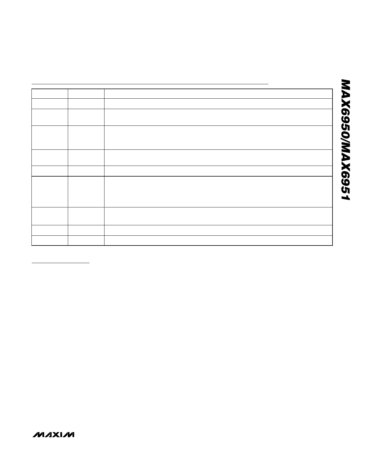
PIN
1
2
3–6, 10–14
7
8
9
15
16
PAD
Pin Description
NAME
FUNCTION
DIN
Serial Data Input. Data is loaded into the internal 16–bit Shift register on CLK’s rising edge.
CLK
Serial-Clock Input. On CLK’s rising edge, data is shifted into the Internal Shift register. On CLK’s
falling edge, data is clocked out of DOUT. CLK input is active only while CS is low.
DIGX, SEGX
Digit X outputs sink current from the display common cathode when acting as digit drivers.
Segment X drivers source current to the display. Segment/digit drivers are high impedance when
turned off.
ISET
GND
Current Setting. Connect to GND through a resistor (RSET) to set the peak current. This resistor,
together with capacitor CSET, also sets the multiplex clock frequency.
Ground
OSC
Multiplexer Clock Input. A capacitor (CSET) is connected to GND when the internal RC oscillator
multiplex clock is used. Resistor RSET (also used to set the peak current) and capacitor CSET
together set the multiplex clock frequency. When the external clock is used, OSC should be driven
by a 1MHz to 8MHz clock.
CS
Chip-Select Input. Serial data is loaded into the Shift register while CS is low. The last 16 bits of
serial data are latched on CS’s rising edge.
V+
Positive Supply Voltage. Bypass to GND with a 0.1µF capacitor.
Exposed pad Exposed pad on package underside. Connect to GND.
Detailed Description
Differences Between
MAX6950 and MAX6951
The MAX6950 is a five-digit common-cathode display
driver. It drives five digits, with each digit comprising
eight LEDs with cathodes connected to a common
cathode. The display limit is therefore 40 LEDs or digit
segments.
The MAX6951 is an eight-digit common-cathode dis-
play driver. It drives eight digits, with each digit com-
prising eight LEDs. The only difference between the
MAX6950 and MAX6951 is that the MAX6950 is missing
three digit drivers. The MAX6950 can be configured to
scan eight digits, but if the last three digits are wired
up, they do not light.
The MAX6950/MAX6951 use a unique multiplexing
scheme to minimize the connections between the driver
and LED display. The scheme requires that the seg-
ment connections are different to each of the five
(MAX6950) or eight (MAX6951) digits (Table 1). This is
shown in the Typical Application Circuit, which uses
single-digit type displays. The MAX6950/MAX6951 are
not intended to drive multidigit display types, which
have the segments internally wired together, unless the
segments are wired with the common cathodes to fol-
low Table 1. The MAX6950/MAX6951 can drive multi-
digit LED displays that have the segments individually
pinned for each digit because then the digits can be
connected together correctly externally, just as if indi-
vidual digits were used.
Serial-Addressing Modes
The microprocessor interface on the MAX6950/
MAX6951 is a SPI-compatible 3-wire serial interface
using three input pins (Figure 1). This interface is used
to write configuration and display data to the MAX6950/
MAX6951. The serial interface data word length is 16
bits, which are labeled D15–D0 (Table 2). D15–D8 con-
tain the command address, and D7–D0 contain the
data. The first bit received is D15, the most-significant
bit (MSB). The three input pins are:
• CLK is the serial clock input, and may idle low or
high at the start and end of a write sequence.
• CS is the MAX6950/MAX6951s’ chip-select input,
and must be low to clock data into the MAX6950/
MAX6951.
• DIN is the serial data input, and must be stable
when it is sampled on the rising edge of the clock.
_______________________________________________________________________________________ 5
Share Link: 