MAX6951EEE 데이터 시트보기 (PDF) - Maxim Integrated
부품명
상세내역
제조사
MAX6951EEE Datasheet PDF : 19 Pages
| |||
Serially Interfaced, +2.7V to +5.5V,
5- and 8-Digit LED Display Drivers
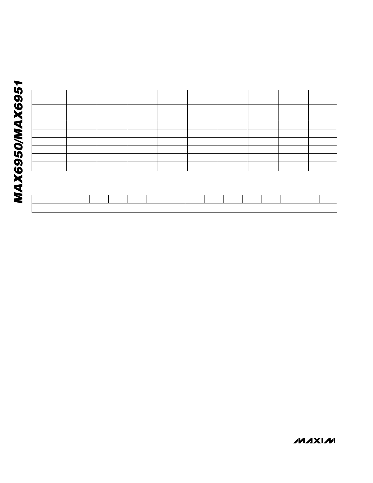
Table 1. Standard Driver Connection to Single-Digit Displays
LED Digit 0
LED Digit 1
LED Digit 2
LED Digit 3
LED Digit 4
LED Digit 5
LED Digit 6
LED Digit 7
DIG/SEG0
PIN 6
CC0
SEG dp
SEG dp
SEG dp
SEG dp
SEG dp
SEG dp
SEG dp
DIG/SEG1
PIN 5
SEG dp
CC1
SEG g
SEG g
SEG g
SEG g
SEG g
SEG g
DIG/SEG2
PIN 4
SEG g
SEG g
CC2
SEG f
SEG f
SEG f
SEG f
SEG f
DIG/SEG3
PIN 3
SEG f
SEG f
SEG f
CC3
SEG e
SEG e
SEG e
SEG e
DIG/SEG4
PIN 14
SEG e
SEG e
SEG e
SEG e
CC4
SEG d
SEG d
SEG d
DIG/SEG5
PIN 13
SEG d
SEG d
SEG d
SEG d
SEG d
CC5
SEG c
SEG c
DIG/SEG6
PIN 12
SEG c
SEG c
SEG c
SEG c
SEG c
SEG c
CC6
SEG b
DIG/SEG7
PIN 11
SEG b
SEG b
SEG b
SEG b
SEG b
SEG b
SEG b
CC7
SEG 8
PIN 10
SEG a
SEG a
SEG a
SEG a
SEG a
SEG a
SEG a
SEG a
Table 2. Serial-Data Format (16 Bits)
D15 D14 D13 D12 D11 D10 D9 D8 D7 D6 D5 D4 D3 D2 D1 D0
ADDRESS
MSB
DATA
LSB
The serial interface comprises a 16-bit shift register into
which DIN data is clocked on the rising edge of CLK
when CS is low. When CS is high, transitions on CLK do
not clock data into the shift register. When CS goes
high, the 16 bits in the shift register are parallel loaded
into a 16-bit latch. The 16 bits in the latch are then
decoded to determine and execute the command.
The MAX6950/MAX6951 are written to using the follow-
ing sequence (Figure 2):
1) Take CLK low.
2) Take CS low. This enables the internal 16-bit shift
register.
3) Clock 16 bits of data in order, D15 first to D0 last,
into DIN, observing the setup and hold times.
4) Take CS high.
CLK and DIN may well be used to transmit data to other
peripherals. The MAX6950/MAX6951 ignore all activity
on CLK and DIN except when CS is low. Data cannot
be read from the MAX6950/MAX6951.
If fewer or greater than 16 bits are clocked into the
MAX6950/MAX6951 between taking CS low and taking
CS high again, the MAX6950/MAX6951 store the last 16
bits received, including the previous transmission(s).
The general case is when n bits (where n > 16) are
transmitted to the MAX6950/MAX6951. The last bits
comprising bits {n-15} to {n} are retained and are paral-
lel loaded into the 16-bit latch as bits D15 to D0,
respectively (Figure 3).
Digit and Control Registers
Table 3 lists the addressable Digit and Configuration
registers. The digit registers are implemented by two
planes of 8-byte dual-port SRAM, P0 and P1.
Initial Power-Up
On initial power-up, all control registers are reset, the
display is blanked, and the MAX6950/MAX6951 enter
shutdown mode. Program the display driver prior to dis-
play use. Otherwise, it is initially set to scan five digits, it
does not decode data in the data registers, and the
Intensity register is set to its minimum value. Table 4
lists the register status after power-up.
Configuration Register
The configuration register is used to enter and exit shut-
down, select the blink rate, globally enable and disable
the blink function, globally clear the digit data, and
reset the blink timing. Bit position D1 should always be
written with a zero when the configuration register is
updated. See Table 5 for configuration register format.
The S bit selects shutdown or normal operation.
The B bit selects the blink rate.
The E bit globally enables or disables the blink function.
The T bit resets the blink timing.
The R bit globally clears the digit data for both planes
P0 and P1 for all digits.
When the MAX6950/MAX6951 are in shutdown mode
(Table 6), the scan oscillator is halted; all segment and
digit drivers are high impedance. Data in the digit and
6 _______________________________________________________________________________________
Share Link: 