MAX6953 데이터 시트보기 (PDF) - Maxim Integrated
부품명
상세내역
제조사
MAX6953 Datasheet PDF : 23 Pages
| |||
2-Wire Interfaced, 2.7V to 5.5V, 4-Digit 5 ✕ 7
Matrix LED Display Driver
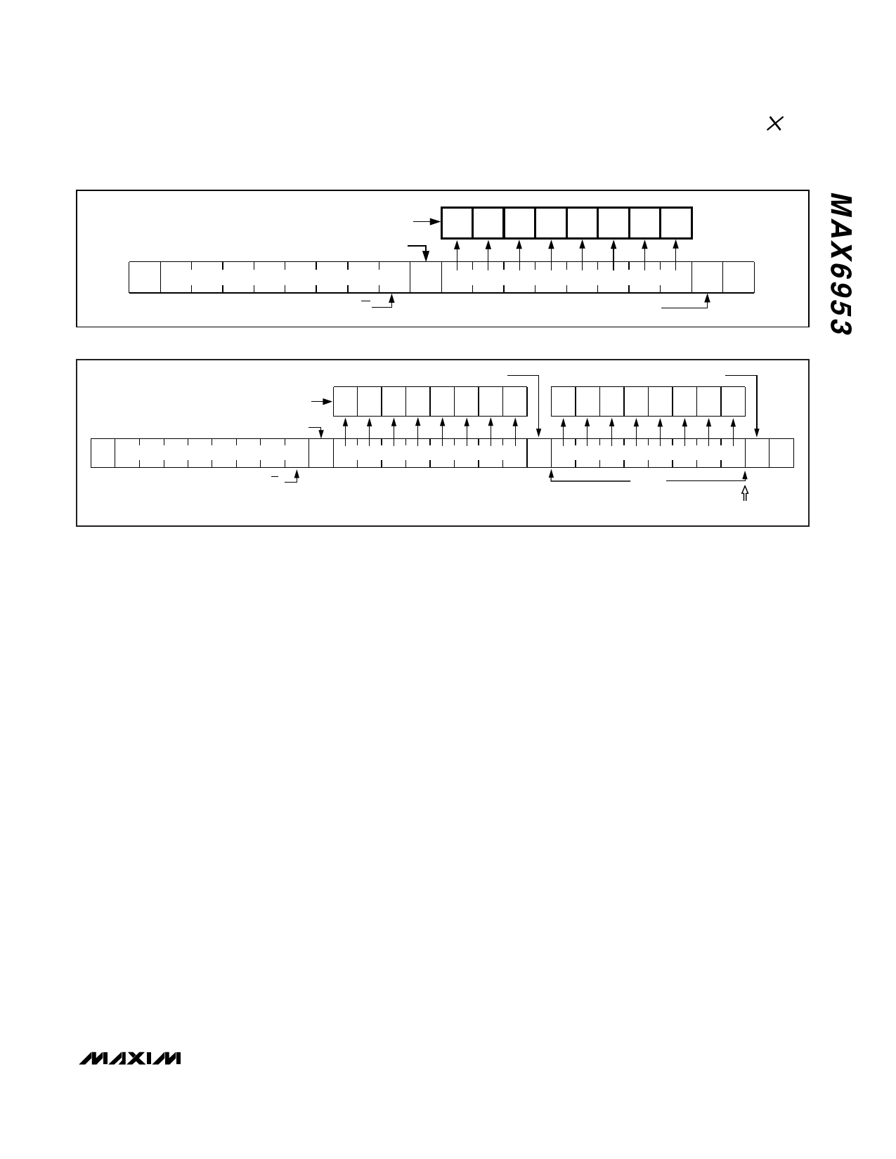
COMMAND BYTE IS STORED ON RECEIPT OF STOP CONDITION
ACKNOWLEDGE FROM MAX6953
D15 D14 D13 D12 D11 D10 D9 D8
S
SLAVE ADDRESS
0A
COMMAND BYTE
AP
R/W
ACKNOWLEDGE FROM MAX6953
Figure 7. Command Byte Received
HOW CONTROL BYTE AND DATA BYTE MAP INTO
MAX6953's REGISTERS
ACKNOWLEDGE FROM MAX6953
ACKNOWLEDGE FROM MAX6953
D15 D14 D13 D12 D11 D10 D9 D8
ACKNOWLEDGE FROM MAX6953
D7 D6 D5 D4 D3 D2 D1 D0
S
SLAVE ADDRESS
0A
COMMAND BYTE
A
DATA BYTE
AP
R/W
1 BYTE
AUTOINCREMENT MEMORY WORD ADDRESS
Figure 8. Command and Single Data Byte Received
read-after-write verification, reset the command byte's
address because the stored byte address generally is
autoincremented after the write (Table 4).
Operation with Multiple Masters
If the MAX6953 is operated on a 2-wire interface with
multiple masters, a master reading the MAX6953
should use a repeated start between the write, which
sets the MAX6953's address pointer, and the read(s)
that takes the data from the location(s). This is because
it is possible for master 2 to take over the bus after
master 1 has set up the MAX6953's address pointer but
before master 1 has read the data. If master 2 subse-
quently changes the MAX6953's address pointer, then
master 1's delayed read may be from an unexpected
location.
Command Address Autoincrementing
Address autoincrementing allows the MAX6953 to be
configured with the shortest number of transmissions
by minimizing the number of times the command byte
needs to be sent. The command address or the font
pointer address stored in the MAX6953 generally incre-
ments after each data byte is written or read (Table 4).
Digit Registers
The MAX6953 uses eight digit registers to store the char-
acters that the user wishes to display on the four 5 ✕ 7
LED digits. These digit registers are implemented with
two planes of 4 bytes, called P0 and P1. Each LED digit
is represented by 2 bytes of memory, 1 byte in plane P0
and the other in plane P1. The digit registers are mapped
so that a digit’s data can be updated in plane P0, or
plane P1, or both planes at the same time (Table 5).
If the blink function is disabled through the Blink Enable
Bit E (Table 10) in the configuration register, then the
digit register data in plane P0 is used to multiplex the
display. The digit register data in P1 is not used. If the
blink function is enabled, then the digit register data in
both plane P0 and plane P1 are alternately used to mul-
tiplex the display. Blinking is achieved by multiplexing
the LED display using data planes P0 and P1 on alter-
nate phases of the blink clock (Table 11).
The data in the digit registers does not control the digit
segments directly. Instead, the register data is used to
address a character generator, which stores the data of
a 128-character font (Table 15). The lower 7 bits of the
digit data (D6 to D0) select the character from the font.
The most-significant bit of the register data (D7) selects
whether the font data is used directly (D7 = 0) or
whether the font data is inverted (D7 = 1). The inversion
feature can be used to enhance the appearance of
bicolor displays by displaying, for example, a red char-
acter on a green background.
Display Blink Mode
The display blinking facility, when enabled, makes the
driver flip automatically between displaying the digit
register data in planes P0 and P1. If the digit register
data for any digit is different in the two planes, then that
_______________________________________________________________________________________ 9
Share Link: 