MAX6954 데이터 시트보기 (PDF) - Maxim Integrated
부품명
상세내역
제조사
MAX6954
Maxim Integrated

MAX6954 Datasheet PDF : 39 Pages
| |||
4-Wire Interfaced, 2.7V to 5.5V LED Display
Driver with I/O Expander and Key Scan
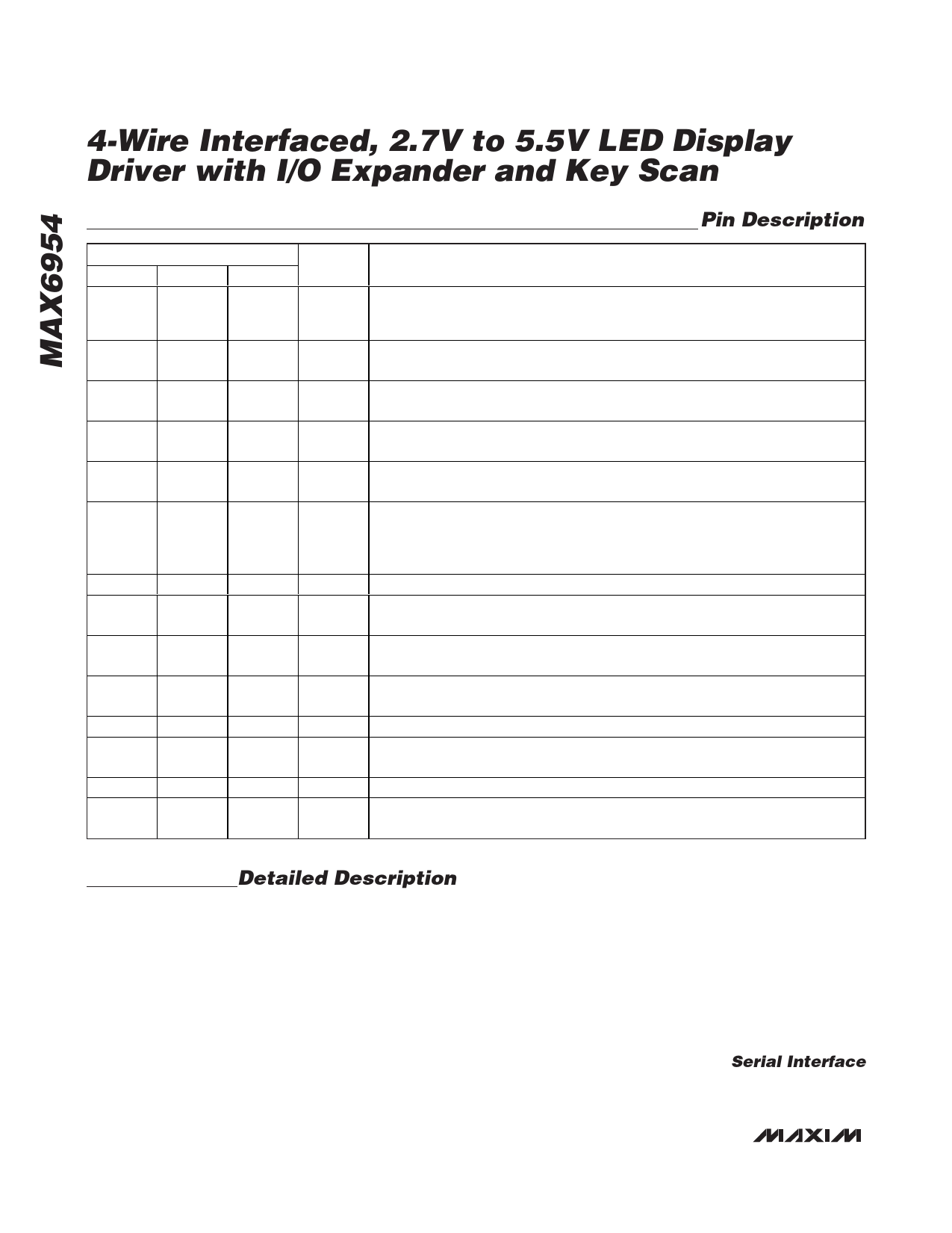
Pin Description
SSOP
PIN
PDIP
T Q F N - EP
1, 2,
1, 2,
36, 37,
34, 35, 36 38, 39, 40 33, 34, 35
3
3
38
NAME
P0–P4
CS
FUNCTION
General-Purpose I/O Ports (GPIOs). GPIO can be configured as logic inputs or
open-drain outputs. Enabling key scanning configures some or all ports P0–P3 as
key-switch matrix inputs with internal pullup and port P4 as IRQ output.
Chip-Select Input. Serial data is loaded into the shift register while CS is low. The
most recent 16 bits of data latch on CS’s rising edge.
4
4
39
DOUT
Serial-Data Output. The data into DIN is valid at DOUT 15.5 clock cycles later. Use
this pin to daisy-chain several devices or allow data readback. Output is push-pull.
5
5
40
CLK
Serial-Clock Input. On CLK’s rising edge, data shifts into the internal shift register. On
CLK’s falling edge, data is clocked out of DOUT. CLK is active only while CS is low.
6
6
1
DIN
Serial-Data Input. Data from DIN loads into the internal 16-bit shift register on CLK’s
rising edge.
7–15,
22–31
7–15,
26–35
2–10,
21–30
O0–O18
Digit/Segment Drivers. When acting as digit drivers, outputs O0 to O7 sink current
from the display common cathodes. When acting as segment drivers, O0 to O18
source current to the display anodes. O0 to O18 are high impedance when not
being used as digit or segment drivers.
16, 18 17, 18, 20 12, 13, 15 GND Ground
17
19
14
ISET
Segment Current Setting. Connect ISET to GND through series resistor RSET to set
the peak current.
Positive Supply Voltage. Bypass V+ to GND with a 47µF bulk capacitor and a 0.1µF
19, 21 21, 23, 24 16, 18, 19
V+
ceramic capacitor.
20
22
17
OSC
Multiplex Clock Input. To use internal oscillator, connect capacitor CSET from OSC
to GND. To use external clock, drive OSC with a 1MHz to 8MHz CMOS clock.
32
36
31
BLINK Blink Clock Output. Output is open drain.
33
37
32
O S C _O U T
Clock Output. OSC_OUT is a buffered clock output to allow easy blink
synchronization of multiple MAX6954s. Output is push-pull.
—
16, 25
11, 20
N.C. Not Connected Internally
—
—
—
EP
Exposed Pad (TQFN package only). Internally connected to GND. Connect to a
large ground plane to maximize thermal performance.
Detailed Description
The MAX6954 is a serially interfaced display driver that
can drive up to 16 digits 7-segment, 8 digits 14-seg-
ment, 8 digits 16-segment, 128 discrete LEDs, or a
combination of these display types. Table 1 shows the
drive capability of the MAX6954 for monocolor and
bicolor displays.
The MAX6954 includes 104-character ASCII font maps
for 14-segment and 16-segment displays, as well as
the hexadecimal font map for 7-segment displays. The
characters follow the standard ASCII font, with the addi-
tion of the following common symbols: £, €, ¥, °, µ, ±,
↑, and ↓. Seven bits represent the 104-character font
map; an 8th bit is used to select whether the decimal
point (DP) is lit. Seven-segment LED digits may be con-
trolled directly or use the hexadecimal font. Direct seg-
ment control allows the MAX6954 to be used to drive
bar graphs and discrete LED indicators.
Tables 2, 3, and 4 list the connection schemes for 16-,
14-, and 7-segment digits, respectively. The letters in
Tables 2, 3, and 4 correspond to the segment labels
shown in Figure 1. (For applications that require mixed
display types, see Tables 37–40.)
Serial Interface
The MAX6954 communicates through an SPI-compati-
ble 4-wire serial interface. The interface has three
6 _______________________________________________________________________________________
Share Link: