MAX9144EUD 데이터 시트보기 (PDF) - Maxim Integrated
부품명
상세내역
제조사
MAX9144EUD Datasheet PDF : 15 Pages
| |||
40ns, Low-Power, 3V/5V, Rail-to-Rail
Single-Supply Comparators
Detailed Description
The MAX9140/MAX9141/MAX9142/MAX9144 single-
supply comparators feature internal hysteresis, high
speed, and low power. Their outputs are pulled to with-
in 300mV of either supply rail without external pullup or
pulldown circuitry. Rail-to-rail input voltage range and
low-voltage single-supply operation make these
devices ideal for portable equipment. The
MAX9140/MAX9141/MAX9142/MAX9144 interface
directly to CMOS and TTL logic.
Most high-speed comparators oscillate in the linear
region because of noise or undesired parasitic feed-
back. This tends to occur when the voltage on one
input is at or equal to the voltage on the other input. To
counter the parasitic effects and noise, the MAX9140/
MAX9141/MAX9142/MAX9144 have an internal hystere-
sis of 1.5mV.
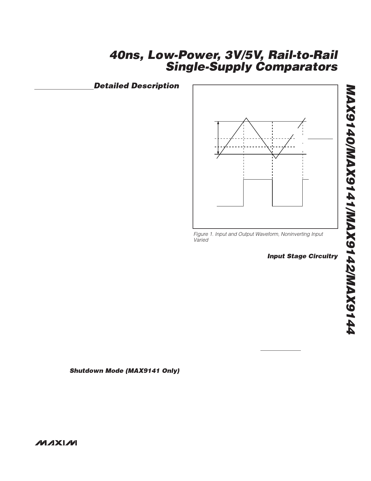
The hysteresis in a comparator creates two trip points:
one for the rising input voltage and one for the falling
input voltage (Figure 1). The difference between the trip
points is the hysteresis. The average of the trip points is
the offset voltage. When the comparator’s input volt-
ages are equal, the hysteresis effectively causes one
comparator input voltage to move quickly past the
other, thus taking the input out of the region where
oscillation occurs. Standard comparators require hys-
teresis to be added with external resistors. The
MAX9140/MAX9141/MAX9142/MAX9144’s fixed internal
hysteresis eliminates these resistors. To increase hys-
teresis and noise margin even more, add positive feed-
back with two resistors as a voltage divider from the
output to the noninverting input.
Figure 1 illustrates the case where IN- is fixed and IN+
is varied. If the inputs were reversed, the figure would
look the same, except the output would be inverted.
iTsnthpoeruatMgimeApXoe9f d1ca4on1mcpein.acrIlifsuL—odEnesirseashnuigltihsn,.tetThrhneealalL—tlEcahtpciihsn
that allows
has a high
transparent
(i.e., the comparator operates as though the latch is not
pwrheesneL—nEt)i.s
The comparator's output
pulled low (Figure 2).
state
is
latched
Shutdown Mode (MAX9141 Only)
The MAX9141 shuts down when the –S—H—D—N– pin is low.
When shut down, the supply current drops to less than
C1ad2nooµwcnAenn,e. wacTntihtdhS—eH—tL—h–DS——EeNH–—htDh—tiogNr–ehVepC-(istnCrtaahnftoeasrpsonauaortpermhnuittagblsheto-acpitnoeepm)r;auetotisotihnmhe.igprEwhexidsiimteas,pnhectuhdete--.
output will be indeterminate.
VTRIP+
VHYST
VTRIP-
COMPARATOR
OUTPUT
VIN+
VOS =
VTRIP+ + VTRIP-
2
VIN- = 0
VOH
VOL
Figure 1. Input and Output Waveform, Noninverting Input
Varied
Input Stage Circuitry
The MAX9140/MAX9141/MAX9142/MAX9144 include
internal protection circuitry that prevents damage to the
precision input stage from large differential input volt-
ages. This protection circuitry consists of two back-to-
back diodes between IN+ and IN- as well as two series
4.1kΩ resistors (Figure 3). The diodes limit the differen-
tial voltage applied to the internal circuitry of the com-
parators to be no more than 2VF, where VF is the for-
ward voltage drop of the diode (about 0.7V at +25°C).
For a large differential input voltage (exceeding 2VF),
this protection circuitry increases the input bias current
at IN+ (source) and IN- (sink).
Input Current = (IN+ - IN-) - 2VF
2 x 4.1kΩ
Input current with large differential input voltages
should not be confused with input bias current (IB). As
long as the differential input voltage is less than 2VF,
this input current is equal to IB. The output is in the cor-
rect logic state if one or both inputs are within the com-
mon-mode range.
_______________________________________________________________________________________ 7
Share Link: 