MAX965 데이터 시트보기 (PDF) - Maxim Integrated
부품명
상세내역
제조사
MAX965 Datasheet PDF : 12 Pages
| |||
Single/Dual/Quad, Micropower,
Ultra-Low-Voltage, Rail-to-Rail I/O Comparators
3) Calculate R1: R1 = (R3 + R4) x (VHB / VCC). Putting
in the values for this example, R1 = (2.2MΩ + 10k) x
(50mV / 5.0V) = 22.1kΩ.
4) Choose the trip point for VIN rising. This is the
threshold voltage where the comparator output tran-
sitions from low to high as VIN rises above the trip
point. For this example, choose 3.0V.
5) Calculate R2 as follows:
R2 =
1
VTHR
VREF x
R1
−
1−
R1
1
R3 + R4
R2 =
1
= 14.76k
3.0V
1.2 x 22k
−
1
22k
−
1
2.2M + 10k
where VTHR is the rising-voltage trip threshold.
Choose a standard value of 15kΩ.
6) Verify trip voltages and hysteresis as follows:
VIN rising:
VTHR
=
VREF
x
R1
x
1
R1
+
1
R2
+
R3
1
+
R4
VIN falling:
VTHF
=
VTHR
−
R1 x
R3 +
VCC
R4
Hysteresis = VTHR − VTHF
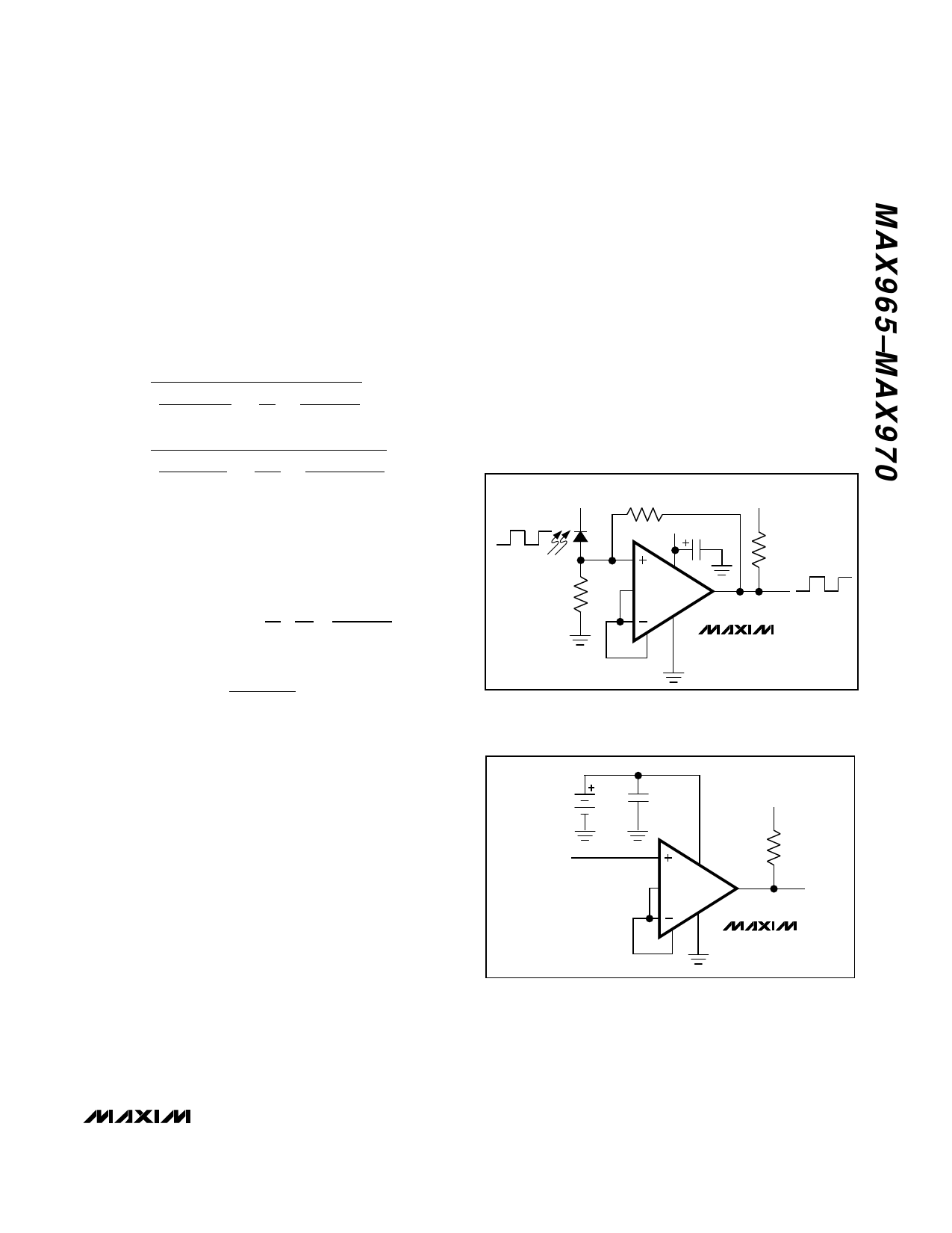
IR Receiver
Figure 5 shows an application using the MAX965 as an
infrared receiver. The infrared photodiode creates a
current relative to the amount of infrared light present.
This current creates a voltage across R1. When this
voltage level crosses the reference voltage applied to
the inverting input, the output transitions. Optional R3
provides additional hysteresis for noise immunity.
2-Cell to TTL Logic-Level Shifter
Figure 6 shows an application using the MAX965
to convert a 2-cell voltage-level signal into a TTL-
compatible signal. The supply voltage for the compara-
tor comes from the 2-cell supply. The output is pulled
up to a 5V supply.
VCC
RD
R3
VCC
0.1µF
VCC
HYST
GND
VCC
RPULL-UP
OUT
REF
MAX965
Figure 5. IR Receiver
where VTHR is the rising-voltage trip point, and VTHF
is the falling-voltage trip point.
Circuit Layout and Bypassing
Power-supply bypass capacitors are not needed if sup-
ply impedance is low, but 100nF bypass capacitors
should be used when supply impedance is high or
when supply leads are long. Minimize signal lead
lengths to reduce stray capacitance between the input
and output that might cause instability.
2 CELLS
INPUT
0.1µF
+5V
VCC
HYST
GND
REF
OUT
MAX965
Figure 6. 2-Cell to TTL Logic-Level Translator
______________________________________________________________________________________ 11
Share Link: 