MAX965 데이터 시트보기 (PDF) - Maxim Integrated
부품명
상세내역
제조사
MAX965 Datasheet PDF : 12 Pages
| |||
Single/Dual/Quad, Micropower,
Ultra-Low-Voltage, Rail-to-Rail I/O Comparators
function below about 1.5V, although the comparators
typically continue to operate with a supply voltage as
low as 1V. At low supply voltages (<1.6V), the input
common-mode range remains rail-to-rail, but the com-
parator’s output sink capability is reduced and propa-
gation delay increases (see Typical Operating
Characteristics).
Figure 1 shows a typical comparator application that
monitors VCC at 1.6V. Resistor divider R1/R2 sets the
voltage trip point (VTRIP) at 1.6V. As VCC drops below
1.6V and approaches 1V, the reference voltage typical-
ly falls below the divider voltage (V+). This causes the
comparator output to change state. If OUT’s state must
be maintained under these conditions, a latching circuit
is required.
Comparator Output
The MAX965–MAX970 contain a unique slew-rate-
controlled output stage capable of rail-to-rail operation
with an external pull-up resistor. Typical comparators
consume orders of magnitude more current during
switching than during steady-state operation. With the
MAX965 family of comparators, during an output transi-
tion from high to low, the output slew rate is limited to
minimize switching current.
Voltage Reference
With VCC greater than 1.6V but less than 5.5V, the inter-
nal 1.235V bandgap reference is ±1.5% accurate over
the commercial temperature range and ±2.5% accu-
rate over the extended temperature range. The REF
output is typically capable of sourcing 50µA. To reduce
reference noise or to provide noise immunity, bypass
REF with a capacitor (0.1nF to 0.1µF).
Noise Considerations
The comparator has an effective wideband peak-to-
peak noise of around 10µV. The voltage reference has
peak-to-peak noise approaching 1.0mV with a 0.1µF
bypass capacitor. Thus, when a comparator is used
with the reference, the combined peak-to-peak noise is
about 1.0mV. This, of course, is much higher than the
individual components’ RMS noise. Avoid capacitive
coupling from any output to the reference pin. Crosstalk
can significantly increase the references’ actual noise.
__________Applications Information
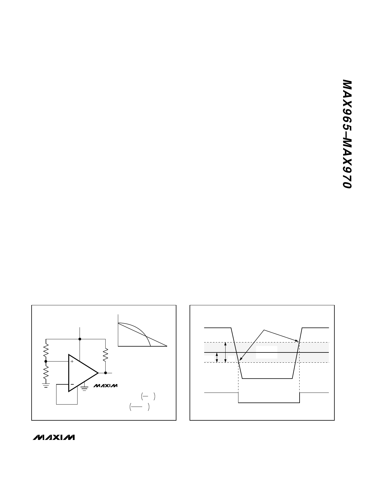
Hysteresis
Many comparators oscillate in the linear region of oper-
ation because of noise or undesired parasitic feed-
back. This tends to occur when the voltage on one
input is equal or very close to the voltage on the other
input. The MAX965–MAX970 have internal hysteresis to
counter parasitic effects and noise. In addition, with the
use of external resistor, the MAX965/MAX967/
MAX968/MAX969’s hysteresis can be programmed to
as much as ±50mV (see the section Adding Hysteresis
to the MAX965/MAX967/MAX968/MAX969).
The hysteresis in a comparator creates two trip points:
one for the rising input voltage and one for the falling
input voltage (Figure 2). The difference between the trip
points is the hysteresis. When the comparator’s input
voltages are equal, the hysteresis effectively causes
one comparator input voltage to move quickly past the
other, thus taking the input out of the region where
oscillation occurs.
R1 47k
V+
R2 150k
VCC
VCC
1.6V
1.0V
V+
VREF
t
100k
VCC
OUT
GND
REF
MAX965
VTRIP = 1.22
R1 = VTRIP
1.22
R1 + 1
R2
- 1 x R2
IN+
IN-
VREF - VHYST
VHB
THRESHOLDS
HYSTERESIS
BAND
OUT
Figure 1. Operation below 1.6V
Figure 2. Threshold Hysteresis Band
_______________________________________________________________________________________ 9
Share Link: 