MAX994ESD 데이터 시트보기 (PDF) - Maxim Integrated
부품명
상세내역
제조사
MAX994ESD Datasheet PDF : 12 Pages
| |||
Micropower, Low-Voltage, UCSP/SC70,
Rail-to-Rail I/O Comparators
5) Calculate R2 as follows. For this example, choose an
8.2kΩ standard value:
R2 =
1
⎛
⎝⎜
VTHR
VREF x
⎞
R1⎠⎟
−
1−
R1
1
R3
R2 =
1
= 8.03kΩ
⎛ 3.0V ⎞
⎝⎜ 1.2 x 12kΩ ⎠⎟
−
1−
12kΩ
1
2.2MΩ
6) Verify trip voltages and hysteresis as follows:
VIN
rising:
VTHR
=
VREF
x
R1 x
⎛1
⎝⎜ R1
+
1
R2
+
1⎞
R3 ⎠⎟
VIN falling:
VTHF =
VTHR
−
⎛ R1
⎝⎜
x VCC
R3
⎞
⎠⎟
Hysteresis = VTHR − VTHF
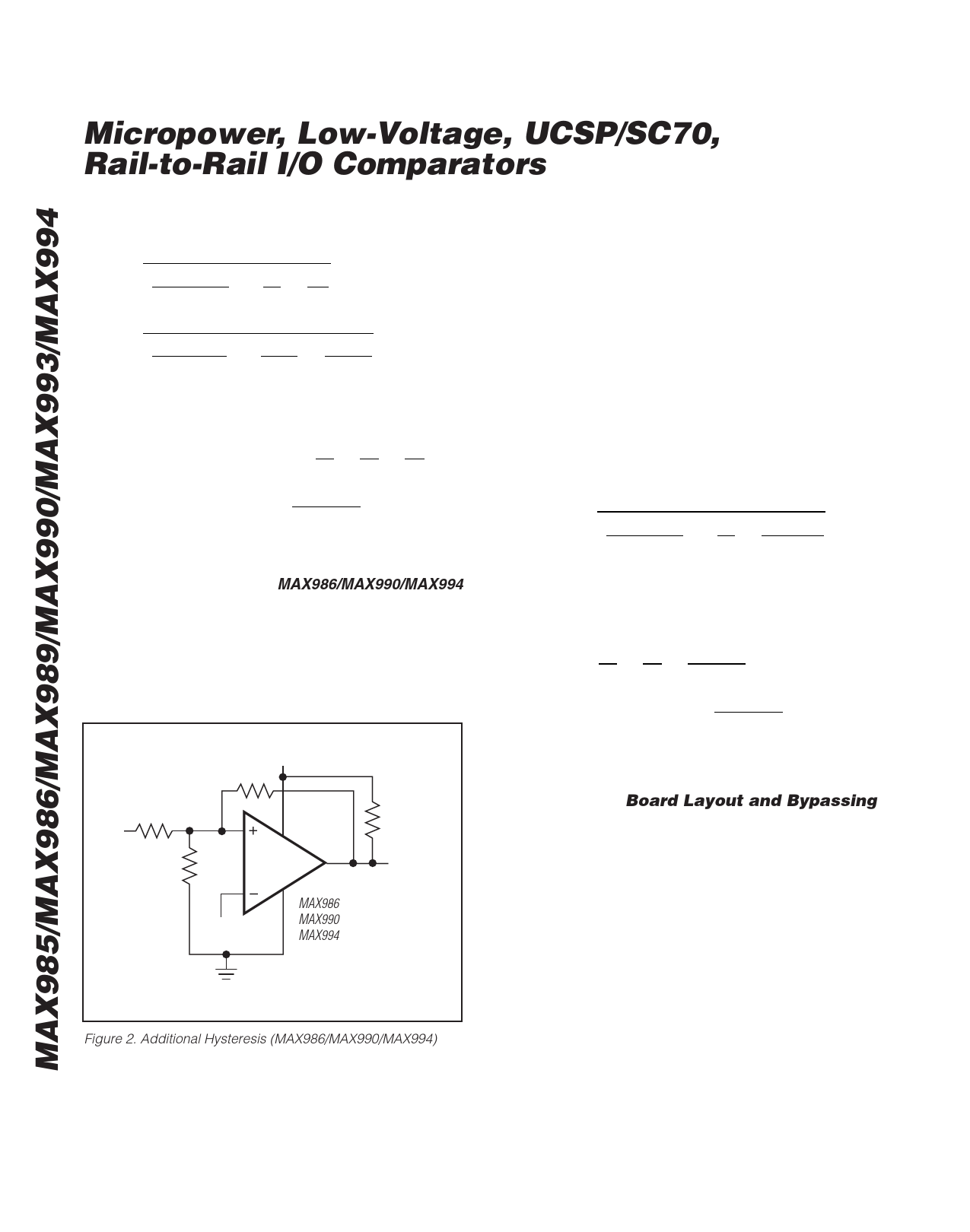
MAX986/MAX990/MAX994
The MAX986/MAX990/MAX994 have ±3mV internal
hysteresis. They have open-drain outputs and require
an external pullup resistor (Figure 2). Additional hys-
teresis can be generated using positive feedback, but
the formulas differ slightly from those of the
MAX985/MAX989/MAX993.
R1
VIN
VCC
R3
R2
VREF
R4
VCC
OUT
VEE
MAX986
MAX990
MAX994
Use the following procedure to calculate resistor
values:
1) Select R3 according to the formulas R3 = VREF /
500µA or R3 = (VREF - VCC) / 500µA - R4. Use the
smaller of the two resulting resistor values.
2) Choose the hysteresis band required (VHB). For this
example, choose 50mV.
3) Calculate R1 according to the following equation:
R1 = (R3 + R4) x (VHB / VCC)
4) Choose the trip point for VIN rising (VTHR; VTHF is
the trip point for VIN falling). This is the threshold
voltage at which the comparator switches its output
from low to high as VIN rises above the trip point.
5) Calculate R2 as follows:
R2 =
1
⎛
⎝⎜
VTHR
VREF x
⎞
R1⎠⎟
−
1−
R1
1
R3 + R4
6) Verify trip voltages and hysteresis as follows:
VIN rising: VTHR = VREF x R1 x
⎛1
⎝⎜ R1
+
1
R2
+
1⎞
R3 + R4⎠⎟
VIN falling:
VTHF =
VTHR
−
⎛
⎝⎜
R1
R3
x
+
VCC
R4
⎞
⎠⎟
Hysteresis = VTHR − VTHF
Board Layout and Bypassing
Power-supply bypass capacitors are not typically need-
ed, but use 100nF bypass capacitors when supply
impedance is high, when supply leads are long,
or when excessive noise is expected on the supply
lines. Minimize signal trace lengths to reduce stray
capacitance.
Figure 2. Additional Hysteresis (MAX986/MAX990/MAX994)
8
Share Link: 