MAX9944(2009) 데이터 시트보기 (PDF) - Maxim Integrated
부품명
상세내역
제조사
MAX9944 Datasheet PDF : 15 Pages
| |||
High-Voltage, Precision, Low-Power Op Amps
MAX9943
6 TDFN-EP
1
—
—
2
3
—
—
4
—
—
5
6
MAX9943
8 µMAX
6
—
—
4
3
—
—
2
—
—
1, 5, 8
7
MAX9944
8 SO/TDFN-EP
—
1
7
4
—
3
5
—
2
6
—
8
—
—
—
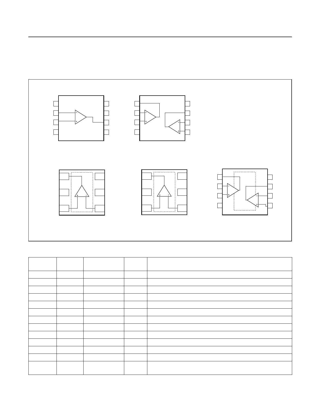
Pin Description
NAME
FUNCTION
OUT
OUTA
OUTB
VEE
IN+
INA+
INB+
IN-
INA-
INB-
N.C.
VCC
EP
Output
Output A
Output B
Negative Power Supply. Bypass with a 0.1µF capacitor to ground.
Positive Input
Positive Input A
Positive Input B
Negative Input
Negative Input A
Negative Input B
No Connection
Positive Power Supply. Bypass with a 0.1µF capacitor to ground.
Exposed Pad (TDFN Only). Connect to a large ground plane to
maximize thermal performance. Not intended as an electrical
connection point.
Detailed Description
The MAX9943/MAX9944 are single/dual operational
amplifiers designed for industrial applications. They
operate from 6V to 38V supply range while maintaining
excellent performance. These devices utilize a three-
stage architecture optimized for low offset voltage and
low input noise with only 550µA supply current. The
devices are unity gain stable with a 1nF capacitive
load. These well-matched devices guarantee the high
open-loop gain, CMRR, PSRR, and low voltage offset.
The MAX9943/MAX9944 provide a wide input/output
voltage range. The input terminals of the MAX9943/
MAX9944 are protected from excessive differential volt-
age with back-to-back diodes. The input signal current
is also limited by an internal series resistor. With a 40V
differential voltage, the input current is limited to 20mA.
The output can swing to the negative rail while deliver-
ing 20mA of current, which is ideal for loop-powered
system applications. The specifications and operation
of the MAX9943/MAX9944 family is guaranteed over the
-40°C to +125°C temperature range.
Application Information
Bias Current vs. Input Common Mode
The MAX9943/MAX9944 use an internal bias current
cancellation circuit to achieve very low bias current over
a wide input common-mode range. For such a circuit to
function properly, the input common mode must be at
least 300mV away from the negative supply VEE. The
input common mode can reach the negative supply
VEE. However, in the region between VEE and VEE +
0.3V, there is an increase in bias current for both inputs.
Capacitive Load Stability
Driving large capacitive loads can cause instability in
many op amps. The MAX9943/MAX9944 are stable with
capacitive loads up to 1nF. The Capacitive Load vs.
Resistive Load graph in the Typical Operating
Characteristics gives the stable operation region for
capacitive versus resistive loads. Stability with higher
capacitive loads can be improved by adding an isola-
tion resistor in series with the op-amp output, as shown
in Figure 1. This resistor improves the circuit’s phase
margin by isolating the load capacitor from the amplifi-
er’s output.
_______________________________________________________________________________________ 7
Share Link: 