MAX9944(2009) 데이터 시트보기 (PDF) - Maxim Integrated
부품명
상세내역
제조사
MAX9944 Datasheet PDF : 15 Pages
| |||
High-Voltage, Precision, Low-Power Op Amps
Power Supplies and Layout
The MAX9943/MAX9944 can operate with dual supplies
from ±3V to ±19V or with a single supply from +6V to
+38V with respect to ground. When used with dual sup-
plies, bypass both VCC and VEE with their own 0.1µF
capacitor to ground. When used with a single supply,
bypass VCC with a 0.1µF capacitor to ground. Careful
layout technique helps optimize performance by
decreasing the amount of stray capacitance at the op
amp’s inputs and outputs. To decrease stray capaci-
tance, minimize trace lengths by placing external com-
ponents close to the op amp’s pins.
Output Current Capability
The MAX9943/MAX9944 are capable of driving heavy
loads such as the ones that can be found in loop-pow-
ered systems for remote sensors. The information is
transmitted through ±20mA or 4mA–20mA current output
across long lines that are terminated with low resistance
loads (e.g., 600Ω). The Typical Application Circuit shows
the MAX9944 used as a voltage-to-current converter with
a current-sense amplifier in the feedback loop. Because
of the high output current capability of the MAX9944, the
device can be used to directly drive the current-loop.
The specifications and operation of the MAX9943/
MAX9944 family is guaranteed over the -40°C to
+125°C temperature range, However, when used in
applications with ±15V supply voltage (see Figure 3),
the capability of driving more than ±20mA of current is
limited to the -40°C to +85°C temperature range. Use a
lower supply voltage if this current must be delivered at
a higher temperature range.
Input Common Mode and Output Swing
The MAX9943/MAX9944 input common-mode range
can swing to the negative rail VEE. The output voltage
can swing to both the positive VCC and the negative
VEE rails if the output stage is not heavily loaded. These
two features are very important for applications where
the MAX9943/ MAX9944 are used with a single-supply
(VEE connected to ground). One of the applications that
can benefit from these features is when the single-sup-
ply op amp is driving an ADC.
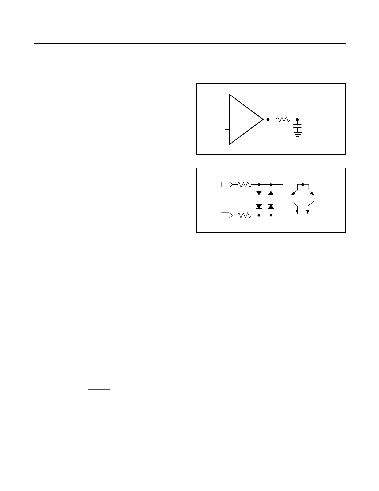
INPUT
MAX9943
RISO
OUTPUT
CL
Figure 1. Capacitive Load Driving Circuit
1.5kΩ
1.5kΩ
Figure 2. Input Protection Circuit
Input Differential Voltage Protection
During normal op-amp operation, the inverting and non-
inverting inputs of the MAX9943/MAX9944 are at essen-
tially the same voltage. However, either due to fast
input voltage transients or due to other fault conditions,
these pins can be forced to be at two different voltages.
Internal back-to-back diodes and series resistors pro-
tect the inputs from an excessive differential voltage
(see Figure 2). Therefore, IN+ and IN- can be any volt-
age within the range shown in the absolute maximum
rating. Note the protection time is still dependent on the
package thermal limits.
Chip Information
PROCESS: BiCMOS
8 _______________________________________________________________________________________
Share Link: 