MAX98302 데이터 시트보기 (PDF) - Maxim Integrated
부품명
상세내역
제조사
MAX98302 Datasheet PDF : 13 Pages
| |||
Stereo 2.4W Class D Amplifier
Detailed Description
The MAX98302 features industry-leading quiescent cur-
rent, low-power shutdown mode, comprehensive click-
and-pop suppression, and excellent RF immunity.
The MAX98302 offers Class AB audio performance with
Class D efficiency in a minimal board-space solution.
The Class D amplifier features spread-spectrum modu-
lation, edge-rate, and overshoot control circuitry that
offers significant improvements to switch-mode amplifier
radiated emissions.
The MAX98302 amplifier features click-and-pop sup-
pression that reduces audible transients on startup and
shutdown. The amplifier includes thermal-overload and
short-circuit protection.
Class D Speaker Amplifier
The MAX98302 filterless Class D amplifier offers much
higher efficiency than Class AB amplifiers. The high
efficiency of a Class D amplifier is due to the switching
operation of the output stage transistors. Any power loss
associated with the Class D output stage is mostly due
to the I2R loss of the MOSFET on-resistance and quies-
cent current overhead.
Ultra-Low-EMI Filterless Output Stage
Traditional Class D amplifiers require the use of external
LC filters, or shielding, to meet EN55022B electromagnet-
ic-interference (EMI) regulation standards. Maxim’s active
emissions limiting edge-rate control circuitry and spread-
spectrum modulation reduce EMI emissions, while main-
taining up to 83% efficiency.
Maxim’s spread-spectrum modulation mode flattens
wideband spectral components, while proprietary tech-
niques ensure that the cycle-to-cycle variation of the
switching period does not degrade audio reproduc-
tion or efficiency. The MAX98302’s spread-spectrum
modulator randomly varies the switching frequency by
Q7kHz around the center frequency (300kHz). Above
10MHz, the wideband spectrum looks like noise for EMI
purposes.
Speaker Current Limit
If the output current of the speaker amplifier exceeds the
current limit (2A typ), the MAX98302 disables the out-
puts for approximately 100Fs. At the end of 100Fs, the
outputs are re-enabled. If the fault condition still exists,
the MAX98302 continues to disable and re-enable the
outputs until the fault condition is removed.
Selectable Gain
The MAX98302 offers five programmable gains selected
using the GAIN input.
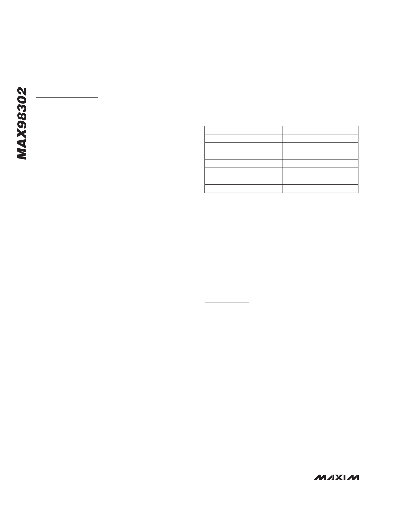
Table 1. Gain Control Configuration
GAIN PIN
MAXIMUM GAIN (dB)
Connect to PGND
18
Connect to PGND through
100kI ±5% resistor
15
Connect to PVDD
12
Connect to PVDD through
100kI ±5% resistor
9
Unconnected
6
Shutdown
The MAX98302 features a low-power shutdown mode,
drawing 0.17FA of supply current. Drive SHDN low to put
the MAX98302 into shutdown.
Click-and-Pop Suppression
The MAX98302 speaker amplifier features Maxim’s com-
prehensive click-and-pop suppression. During startup,
the click-and-pop suppression circuitry reduces any
audible transient sources internal to the device. When
entering shutdown, the differential speaker outputs ramp
down to PGND quickly and simultaneously.
Applications Information
Filterless Class D Operation
Traditional Class D amplifiers require an output filter. The
filter adds cost and size and decreases THD+N perfor-
mance. The MAX98302’s filterless modulation scheme
does not require an output filter.
Because the switching frequency of the MAX98302 is
well beyond the bandwidth of most speakers, voice coil
movement due to the switching frequency is very small.
Use a speaker with a series inductance > 10FH. Typical
8I speakers exhibit series inductances in the 20FH to
100FH range.
Component Selection
Speaker Amplifier Power-Supply Input (PVDD)
PVDD powers the speaker amplifier. PVDD ranges from
2.6V to 5.5V. Bypass PVDD with 0.1FF and 10FF capaci-
tors to PGND. Also, connect at least 10FF of system bulk
capacitance to PVDD. Apply additional bulk capaci-
tance at the device if long input traces between PVDD
and the power source are used.
8 _______________________________________________________________________________________
Share Link: 