MB90F543 데이터 시트보기 (PDF) - Fujitsu
부품명
상세내역
제조사
MB90F543 Datasheet PDF : 67 Pages
| |||
MB90540/540G/545/545G Series
s HANDLING DEVICES
(1) Preventing latch-up
CMOS IC chips may suffer latch-up under the following conditions :
• A voltage higher than VCC or lower than VSS is applied to an input or output pin.
• A voltage higher than the rated voltage is applied between VCC and VSS.
• The AVcc power supply is applied before the VCC voltage.
Latch-up may increase the power supply current drastically, causing thermal damage to the device.
For the same reason, care must also be taken in not allowing the analog power-supply voltage (AVCC, AVRH) to
exceed the digital power-supply voltage.
(2) Handling unused pins
Leaving unused input pins open may result in misbehavior or latch up and possible permanent damage of the
device. Therefor they must be pulled up or pulled down through resistors. In this case those resistors should be
more than 2 kΩ.
Unused bi-directional pins should be set to the output state and can be left open, or the input state with the
above described connection.
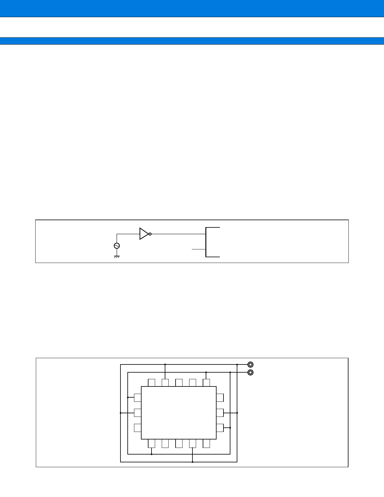
(3) Using external clock
To use external clock, drive X0 pin only and leave X1 pin unconnected.
Below is a diagram of how to use external clock.
MB90540/545 Series
X0
Open
X1
(4) Use of the sub-clock
Use one clock system parts when the sub-clock is not used. In that case, pull-down the pin X0A and leave the
pin X1A open. When using two clock system parts, a 32 kHz oscillator has to be connected to the X0A and X1A
pins.
(5) Power supply pins (VCC/VSS)
In products with multiple VCC or VSS pins, the pins of a same potential are internally connected in the device to
avoid abnormal operations including latch-up. However you must connect the pins to an external power and a
ground line to lower the electro-magnetic emission level to prevent abnormal operation of strobe signals caused
by the rise in the ground level, and to conform to the total current rating.
Make sure to connect VCC and VSS pins via the lowest impedance to power lines.
It is recommended to provide a bypass capacitor of around 0.1 µF between VCC and VSS pins near the device.
VCC
VSS
VSS
VCC
VSS
VCC
MB90540/545
VCC
Series
VSS
VCC
VSS
17
Share Link: 