MB90F543 데이터 시트보기 (PDF) - Fujitsu
부품명
상세내역
제조사
MB90F543 Datasheet PDF : 67 Pages
| |||
MB90540/540G/545/545G Series
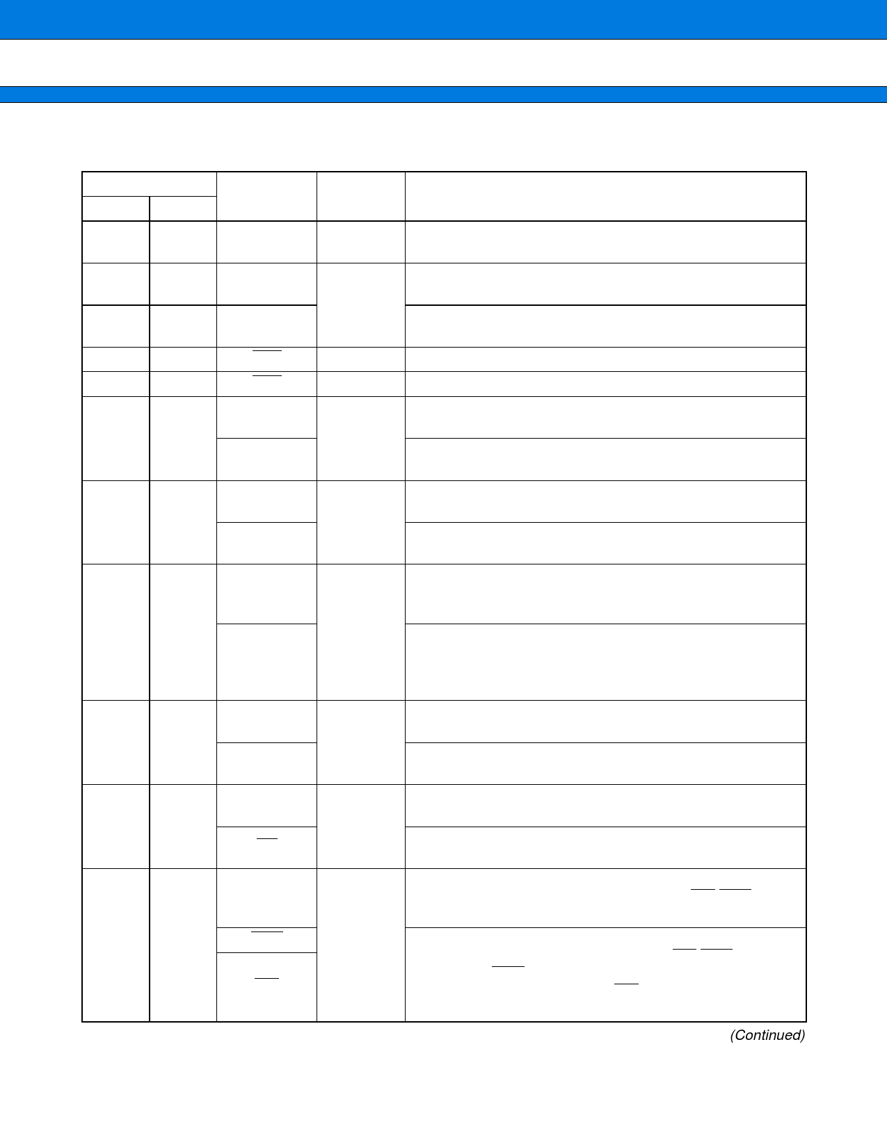
s PIN DESCRIPTION
Pin No.
LQFP*2 QFP*1
Pin name Circuit type
Function
80
82
81
83
X0
X1
A
(Oscillation)
High speed crystal oscillator input pins
78
80
77
79
X0A
Low speed crystal oscillator input pins. For the one clock sys-
A
tem parts, perfom external pull-down processing.
X1A
(Oscillation) Low speed crystal oscillator input pins. For the one clock sys-
tem parts, leave it open.
75
77
RST
B
External reset request input pin
50
52
HST
C
Hardware standby input pin
P00 to P07
General I/O port with programmable pullup. This function is
enabled in the single-chip mode.
83 to 90 85 to 92
I
AD00 to AD07
I/O pins for 8 lower bits of the external address/data bus. This
function is enabled when the external bus is enabled.
P10 to P17
General I/O port with programmable pullup. This function is
enabled in the single-chip mode.
91 to 98 93 to 100
I
AD08 to AD15
I/O pins for 8 higher bits of the external address/data bus. This
function is enabled when the external bus is enabled.
P20 to P27
99 to 6
1 to 8
A16 to A23
General I/O port with programmable pullup. In external bus
mode, this function is valid when the corresponding bits in the
external address output control resister (HACR) are set to “1”.
I
8-bit I/O pins for A16 to A23 at the external address/data bus.
In external bus mode, this function is valid when the corre-
sponding bits in the external address output control resister
(HACR) are set to “0”.
P30
7
9
ALE
General I/O port with programmable pullup. This function is
enabled in the single-chip mode.
I
Address latch enable output pin. This function is enabled
when the external bus is enabled.
P31
8
10
RD
General I/O port with programmable pullup. This function is
enabled in the single-chip mode.
I
Read strobe output pin for the data bus. This function is en-
abled when the external bus is enabled.
General I/O port with programmable pullup. This function is
P32
enabled in the single-chip mode or when the WR/WRL pin out-
put is disabled.
10
12
WRL
WR
I
Write strobe output pin for the data bus. This function is en-
abled when both the external bus and the WR/WRL pin output
are enabled. WRL is write-strobe output pin for the lower 8 bits
of the data bus in 16-bit access. WR is write-strobe output pin
for the 8 bits of the data bus in 8-bit access.
(Continued)
9
Share Link: 