MB91354A 데이터 시트보기 (PDF) - Fujitsu
부품명
상세내역
제조사
MB91354A Datasheet PDF : 111 Pages
| |||
MB91350A Series
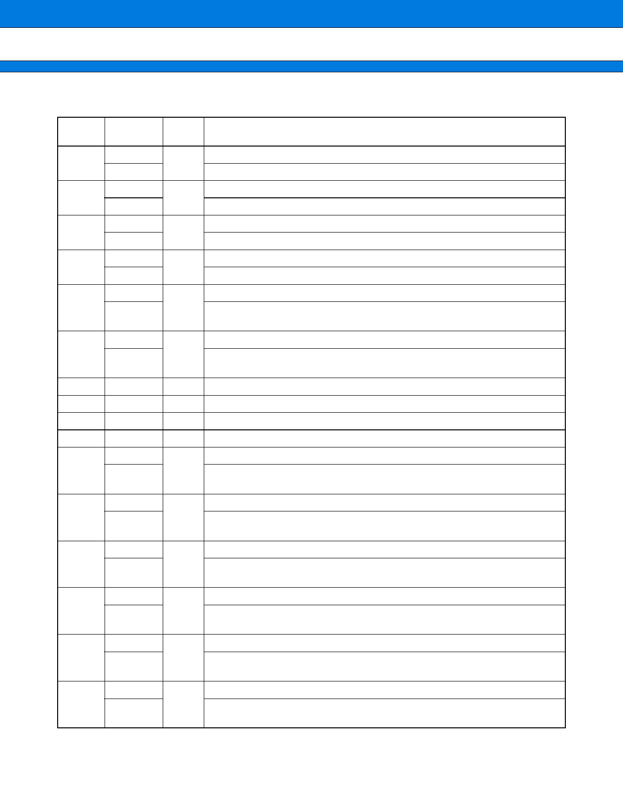
■ PIN DESCRIPTION
Pin no.
Pin name
Circuit
type
Description
D16 to D23
External data bus bit 16 to bit 23. Enabled in external bus mode.
1 to 8
C
P20 to P27
Available as a port in external bus 8-bit mode.
D24 to D31
external data bus bit 24 to bit 31. Enabled in external bus mode.
9 to 16
C
P30 to P37
Usable as port at single chip mode.
A00 to A07
19 to 26
P40 to P47
Bits 0 to 7 of external address bus. Enabled in external bus mode.
C
Usable as port at single chip mode.
A08 to A15
27 to 34
P50 to P57
Bits 8 to 15 of external address bus. Enabled in external bus mode.
C
Usable as port at single chip mode.
A16 to A20
37 to 41
P60 to P64
Bits 16 to 20 of external address bus. Enabled in external bus mode.
C Available as a port either in single chip mode or with no external address bus in
use.
A21 to A23
42 to 44
P65 to P67
Bits 21 to 23 of external address bus. Enabled in external bus mode.
C Available as a port either in single chip mode or with no external address bus in
use.
47 to 48 DA0, DA1 ⎯ D/A converter output pin.
49
DA2
⎯ D/A converter output pin.
50 to 57 AN0 to AN7 G Analog input pin.
58 to 61 AN8 to AN11 G Analog input pin.
TOT0 to TOT3
Reload timer output port. This function is enabled when timer output is enabled.
67 to 70
PP0 to PP3
D
General purpose input/output port. This function is enabled when the timer out-
put function is disabled.
OC0
Output compare pin.
71
PO0
D General purpose I/O. This function is available as a port when the output com-
pare output is not in use.
OC1
Output compare pin.
72
PO1
D General purpose I/O. This function is available as a port when the output com-
pare output is not in use.
OC2
Output compare pin.
73
PO2
D General purpose I/O. This function is available as a port when the output com-
pare output is not in use.
OC3 to OC7
Output compare pin.
74 to 78
PO3 to PO7
D
General purpose I/O. This function is available as a port when the output com-
pare output is not in use.
PPG0
PPG timer output pin.
81
PN0
D General purpose I/O. This function is available as a port when the PPG timer out-
put is not in use.
(Continued)
5
Share Link: 