MC100LVEL33 데이터 시트보기 (PDF) - ON Semiconductor
부품명
상세내역
제조사
MC100LVEL33 Datasheet PDF : 8 Pages
| |||
MC100LVEL33
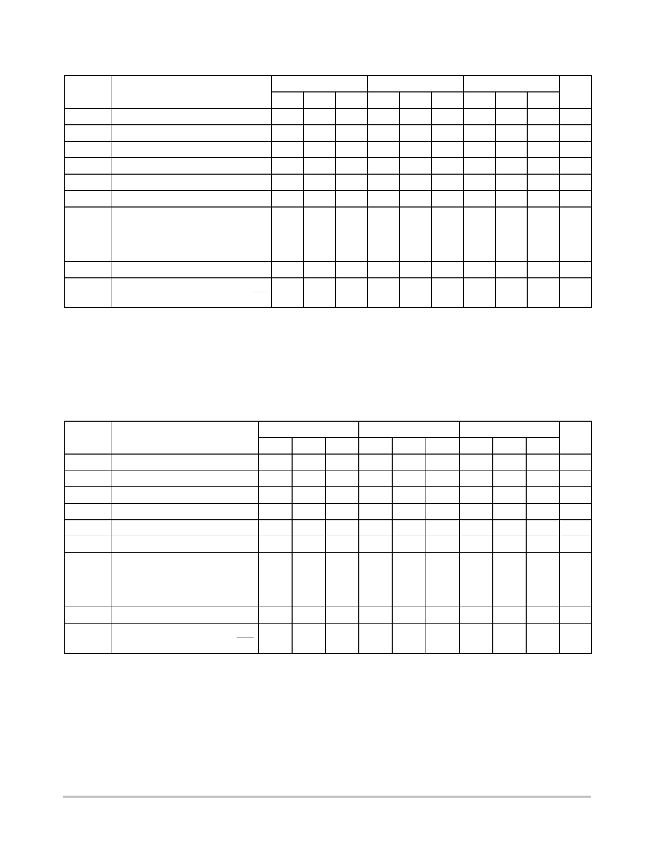
Table 3. LVPECL DC CHARACTERISTICS VCC = 3.3 V; VEE = 0.0 V (Note 1)
−40°C
25°C
85°C
Symbol
Characteristic
Min Typ Max Min Typ Max Min Typ Max Unit
IEE
VOH
VOL
VIH
VIL
VBB
VIHCMR
Power Supply Current
33
37
33
37
35
39 mA
Output HIGH Voltage (Note 2)
2215 2295 2420 2275 2345 2420 2275 2345 2420 mV
Output LOW Voltage (Note 2)
1470 1605 1745 1490 1595 1680 1490 1595 1680 mV
Input HIGH Voltage (Single−Ended)
2135
2420 2135
2420 2135
2420 mV
Input LOW Voltage (Single−Ended)
1490
1825 1490
1825 1490
1825 mV
Output Voltage Reference
1.92
2.04 1.92
2.04 1.92
2.04 V
Input HIGH Voltage Common Mode
Range (Differential) (Note 6)
VPP < 500 mV 1.2
VPP y 500 mV 1.4
2.9 1.1
2.9 1.3
2.9 1.1
2.9 1.3
2.9
V
2.9
V
IIH
Input HIGH Current
IIL
Input LOW Current
Other 0.5
CLK −600
150
0.5
−600
150
0.5
−600
150 mA
mA
mA
NOTE: Device will meet the specifications after thermal equilibrium has been established when mounted in a test socket or printed circuit
board with maintained transverse airflow greater than 500 lfpm. Electrical parameters are guaranteed only over the declared
operating temperature range. Functional operation of the device exceeding these conditions is not implied. Device specification limit
values are applied individually under normal operating conditions and not valid simultaneously.
1. Input and output parameters vary 1:1 with VCC. VEE can vary ±0.3 V.
2. Outputs are terminated through a 50 W resistor to VCC − 2.0 V.
3. VIHCMR min varies 1:1 with VEE, max varies 1:1 with VCC. The VIHCMR range is referenced to the most positive side of the differential input signal.
Normal operation is obtained if the HIGH level falls within the specified range and the peak-to-peak voltage lies between VPPmin and 1 V.
Table 4. LVNECL DC CHARACTERISTICS VCC = 0.0 V; VEE = −3.3 V (Note 4)
−40°C
25°C
85°C
Symbol
Characteristic
Min Typ Max Min Typ Max Min Typ Max Unit
IEE
VOH
VOL
VIH
VIL
VBB
VIHCMR
Power Supply Current
33
37
33
37
35
39 mA
Output HIGH Voltage (Note 5)
−1085 −1005 −880 −1025 −955 −880 −1025 −955 −880 mV
Output LOW Voltage (Note 5)
−1830 −1695 −1555 −1810 −1705 −1620 −1810 −1705 −1620 mV
Input HIGH Voltage (Single−Ended) −1165
−880 −1165
−880 −1165
−880 mV
Input LOW Voltage (Single−Ended) −1810
−1475 −1810
−1475 −1810
−1475 mV
Output Voltage Reference
−1.38
−1.26 −1.38
−1.26 −1.38
−1.26 V
Input HIGH Voltage Common Mode
Range (Differential) (Note 6)
VPP < 500 mV
VPP y 500 mV
−2.1
−1.9
−0.4 −2.2
−0.4 −2.0
−0.4 −2.2
−0.4 −2.0
−0.4 V
−0.4 V
IIH
Input HIGH Current
IIL
Input LOW Current
Other 0.5
CLK −600
150
0.5
−600
150
0.5
−600
150 mA
mA
mA
NOTE: Device will meet the specifications after thermal equilibrium has been established when mounted in a test socket or printed circuit
board with maintained transverse airflow greater than 500 lfpm. Electrical parameters are guaranteed only over the declared
operating temperature range. Functional operation of the device exceeding these conditions is not implied. Device specification limit
values are applied individually under normal operating conditions and not valid simultaneously.
4. Input and output parameters vary 1:1 with VCC. VEE can vary ±0.3 V.
5. Outputs are terminated through a 50 W resistor to VCC − 2.0 V.
6. VIHCMR min varies 1:1 with VEE, max varies 1:1 with VCC. The VIHCMR range is referenced to the most positive side of the differential input signal.
Normal operation is obtained if the HIGH level falls within the specified range and the peak-to-peak voltage lies between VPPmin and 1 V.
http://onsemi.com
3
Share Link: 