MC100LVEL34(2014) 데이터 시트보기 (PDF) - ON Semiconductor
부품명
상세내역
제조사
MC100LVEL34 Datasheet PDF : 9 Pages
| |||
MC100LVEL34
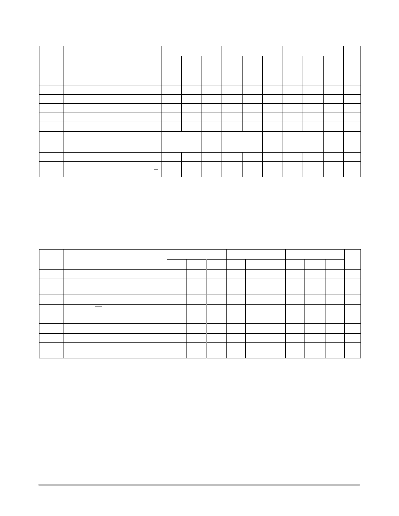
Table 6. 100LVEL DC CHARACTERISTICS, NECL VCC = 0 V, VEE = −3.8 V to −3.0 V (Note 5)
−40°C
25°C
85°C
Symbol
Characteristic
Min Typ Max Min Typ Max Min Typ Max Unit
IEE
IEE
VOH
VOL
VIH
VIL
VBB
VIHCMR
Power Supply Current
Power Supply Current
Output HIGH Voltage (Note 6)
Output LOW Voltage (Note 6)
Input HIGH Voltage (Single−Ended)
Input LOW Voltage (Single−Ended)
Output Voltage Reference
Input HIGH Voltage Common Mode
Range (Differential Configuration)
(Note 7)
23
30
40
23
30
40
23
30
40 mA
40
50
60
40
50
60
42
52
62 mA
−1145 −1020 −895 −1145 −1020 −895 −1145 −1020 −895 mV
−1995 −1700 −1575 −1995 −1700 −1575 −1995 −1700 −1575 mV
−1225
−880 −1225
−880 −1225
−880 mV
−1995
−1625 −1995
−1625 −1995
−1625 mV
−1525 −1425 −1325 −1525 −1425 −1325 −1525 −1425 −1325 mV
VEE + 1.2
0.0
VEE + 1.2
0.0
VEE + 1.2
0.0 V
IIH
Input HIGH Current
IIL
Input LOW Current
D 0.5
D −150
150
0.5
−150
150
0.5
−150
150 mA
mA
NOTE: Device will meet the specifications after thermal equilibrium has been established when mounted in a test socket or printed circuit
board with maintained transverse airflow greater than 500 lfpm. Electrical parameters are guaranteed only over the declared
operating temperature range. Functional operation of the device exceeding these conditions is not implied. Device specification limit
values are applied individually under normal operating conditions and not valid simultaneously.
5. Input and output parameters vary 1:1 with VCC.
6. All loading with 50 W to VCC − 2.0 V.
7. VIHCMR min varies 1:1 with VEE, VIHCMR max varies 1:1 with VCC. The VIHCMR range is referenced to the most positive side of the differential
input signal.
Table 7. AC CHARACTERISTICS VCC = 0 V; VEE = −3.0 V to −5.5 V or VCC = 3.0 V to 5.5 V; VEE = 0 V (Note 8)
−40°C
25°C
85°C
Symbol
Characteristic
Min
fmax
Maximum Toggle Frequency (Figure 4)
1.5
tPLH
Propagation
tPHL
Delay to Output
CLK to Q0, Q1, Q2 550
MR to Q 500
tJITTER Cycle−to−Cycle Jitter (Figure 4)
tS
Setup Time EN
150
tH
Hold Time EN
200
tRR
Set/Reset Recovery
300
VPP
Input Swing (Note 9)
150
tr
Output Rise/Fall Times Q
120
tf
(20% − 80%)
Typ Max Min
1.5
650 1000 600
600 1000 550
<1
50
150
100
200
200
300
1000 150
170 400 140
Typ Max Min
1.5
700 1000 650
650 1000 600
<1
50
150
100
200
200
300
1000 150
180 400 160
Typ Max Unit
GHz
750 1000 ps
700 1000
<1
ps
50
ps
100
ps
200
ps
1000 mV
200 400 ps
NOTE: Device will meet the specifications after thermal equilibrium has been established when mounted in a test socket or printed circuit
board with maintained transverse airflow greater than 500 lfpm. Electrical parameters are guaranteed only over the declared
operating temperature range. Functional operation of the device exceeding these conditions is not implied. Device specification limit
values are applied individually under normal operating conditions and not valid simultaneously.
8. Measured using a 750 mV source, 50% duty cycle clock source. All loading with 50 W to VCC − 2.0 V.
9. VPP(min) is minimum input swing for which AC parameters guaranteed. The device has a DC gain of [40.
Product parametric performance is indicated in the Electrical Characteristics for the listed test conditions, unless otherwise noted. Product
performance may not be indicated by the Electrical Characteristics if operated under different conditions.
http://onsemi.com
4
Share Link: 