MC10E1651(2002) 데이터 시트보기 (PDF) - ON Semiconductor
부품명
상세내역
제조사
MC10E1651 Datasheet PDF : 12 Pages
| |||
MC10E1651
APPLICATIONS INFORMATION
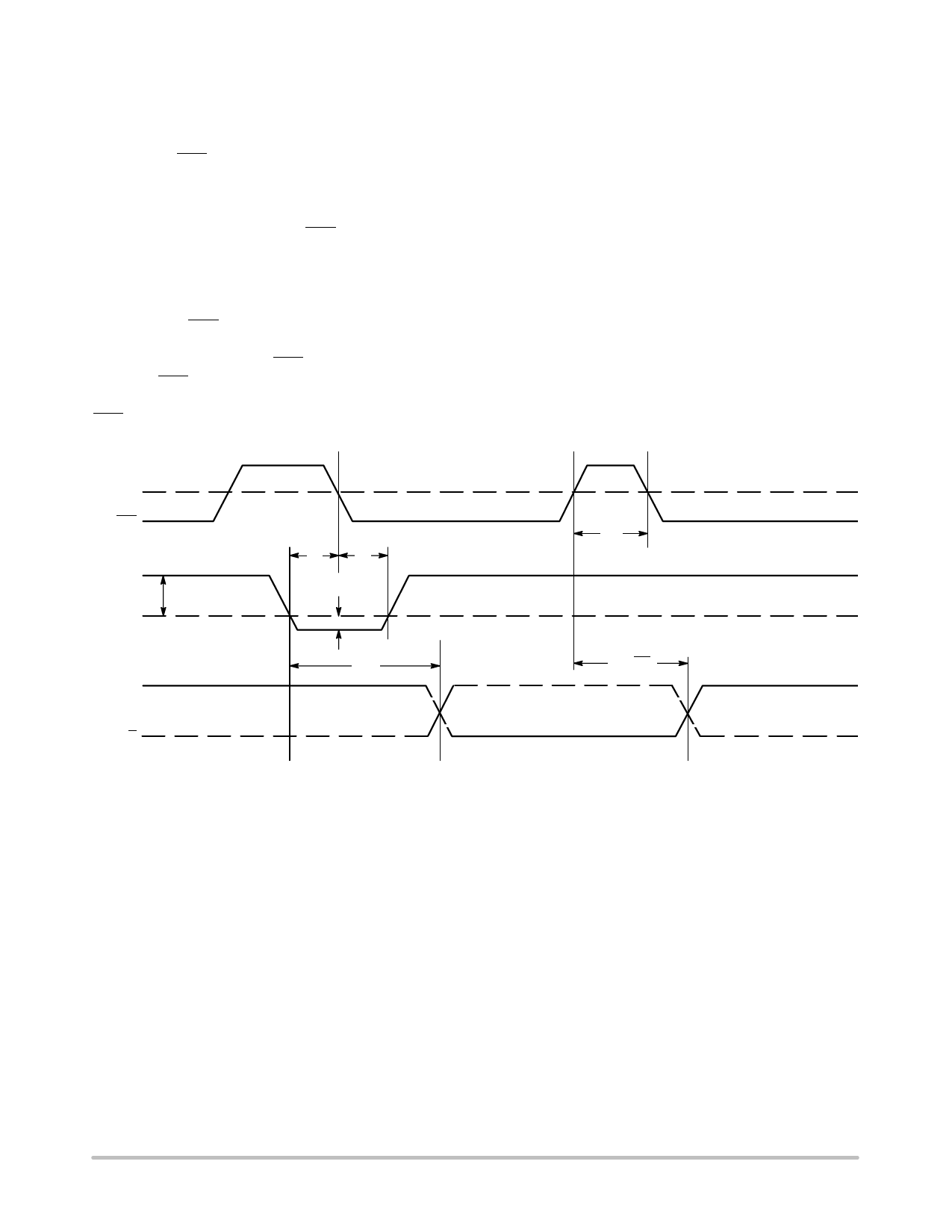
The timing diagram (Figure 3.) is presented to illustrate
the MC10E1651’s compare and latch features. When the
signal on the LEN pin is at a logic high level, the device is
operating in the “compare mode,” and the signal on the input
arrives at the output after a nominal propagation delay (tPHL,
tPLH). The input signal must be asserted for a time, ts, prior
to the negative going transition on LEN and held for a time,
th, after the LEN transition. After time th, the latch is
operating in the “latch mode,” thus transitions on the input
do not appear at the output. The device continues to operate
in the “latch mode” until the latch is asserted once again.
Moreover, the LEN pulse must meet the minimum pulse
width (tpw) requirement to effect the correct input-output
relationship. Note that the LEN waveform in Figure 3.
shows the LEN signal swinging around a reference labeled
VBBINT; this waveform emphasizes the requirement that
LEN follow typical ECL 10KH logic levels because
VBBINT is the internally generated reference level, hence is
nominally at the ECL VBB level.
Finally, VOD is the input voltage overdrive and represents
the voltage level beyond the threshold level (VTHR) to which
the input is driven. As an example, if the threshold level is
set on one of the comparator inputs as 80 mV and the input
signal swing on the complementary input is from zero to
100mV, the positive going overdrive would be 20 mV and
the negative going overdrive would be 80mV. The result of
differing overdrive levels is that the devices have shorter
propagation delays with greater overdrive because the
threshold level is crossed sooner than the case of lower
overdrive levels. Typically, semiconductor manufactures
refer to the threshold voltage as the input offset voltage
(VOS) since the threshold voltage is the sum of the
externally supplied reference voltage and inherent device
offset voltage.
VBBINT
LEN
V
VIN
VTHR
Q
Q
ts
th
VOD
tPHL
tpw
tPLH(LEN)
Figure 3. Input/Output Timing Diagram
http://onsemi.com
5
Share Link: 