MC10E1652(2013) 데이터 시트보기 (PDF) - ON Semiconductor
부품명
상세내역
제조사
MC10E1652 Datasheet PDF : 9 Pages
| |||
MC10E1652
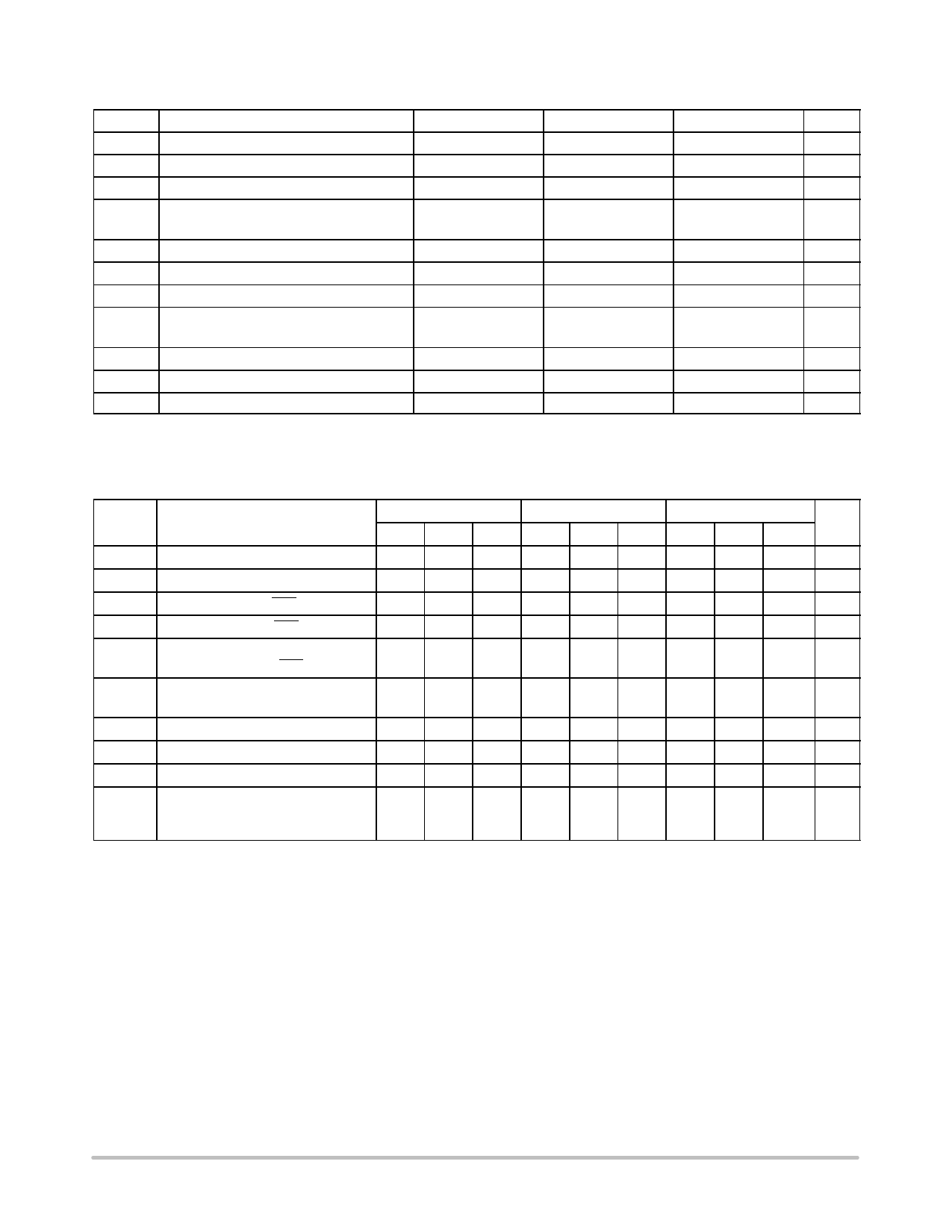
Table 3. MAXIMUM RATINGS
Symbol
Parameter
Condition 1
Condition 2
Rating
Units
VSUP
VPP
Total Supply Voltage
Differential Input Voltage
|VEE| + |VCC|
|V1 − V2|
12.0
V
3.7
V
VI
Input Voltage
Iout
Output Current
Continuous
Surge
VEE v VI v VCC
V
50
mA
100
mA
IBB
VBB Sink/Source
TA
Operating Temperature Range
± 0.5
mA
0 to +85
°C
Tstg
Storage Temperature Range
qJA
Thermal Resistance (Junction to Ambient) 0 LFPM
500 LFPM
28 PLCC
28 PLCC
−65 to +150
63.5
43.5
°C
°C/W
°C/W
qJC
Thermal Resistance (Junction to Case)
std bd
28 PLCC
22 to 26
°C/W
VEE
Operating Range
GND = 0 V
−4.2 to −5.7
V
Tsol
Wave Solder
Pb−Free v 3 sec @ 260°C
265
°C
Stresses exceeding Maximum Ratings may damage the device. Maximum Ratings are stress ratings only. Functional operation above the
Recommended Operating Conditions is not implied. Extended exposure to stresses above the Recommended Operating Conditions may affect
device reliability.
Table 4. DC CHARACTERISTICS VCC = +5.0 V ±5%; VEE = −5.2 V ±5%, VCC = 0 V (Note 1)
0°C
25°C
85°C
Symbol
Characteristic
Min Typ Max Min Typ Max Min Typ Max Unit
VOH
Output HIGH Voltage (Note 2)
VOL
Output Low Voltage (Note 2)
VIL
Input LOW Voltage (LEN)
VIH
Input HIGH Voltage (LEN)
II
Input Current (V1, V2)
IIH
Input HIGH Current (LEN)
−1020
−1950
−1.95
−1.17
−840 −980
−1630 −1950
−1.48 −1.95
−0.84 −1.13
65
150
−810 −920
−1630 −1950
−1.48 −1.95
−0.81 −1.07
65
150
−735 mV
−1600 mV
−1.45 mV
−0.735 mV
65
mA
150
ICC
Positive Supply Current
IEE
Negative Supply Current
50
50
50
mA
−55
−55
−55
VCMR Common Mode Range (Note 3)
−2.0
3.0 −2.0
3.0 −2.0
3.0
V
Hys
Hysteresis (Note 4)
27
27
30
mV
Vskew
Cin
Hysteresis Skew (Note 5)
Input Capacitance
PLCC
−1.0
2
−1.0
2
0
mV
2
pF
NOTE: Device will meet the specifications after thermal equilibrium has been established when mounted in a test socket or printed circuit
board with maintained transverse airflow greater than 500 lfpm. Electrical parameters are guaranteed only over the declared
operating temperature range. Functional operation of the device exceeding these conditions is not implied. Device specification limit
values are applied individually under normal operating conditions and not valid simultaneously.
1. Input VIL and VIH parameters vary 1:1 with VCC. Output VOH and VOL parameters vary 1:1 with GND.
2. Outputs are terminated through a 50 ohm resistor to GND−2 volts.
3. VCMR Min varies 1:1 with VEE; Max varies 1:1 with VCC.
4. The HYS pin programming characterization information is shown in Figure 2. The hysteresis values indicated in the data sheet are for the
condition in which the voltage on the HYS pin is set to VEE.
5. Hysteresis skew (Vskew) is provided to indicate the offset of the hysteresis window. For example, at 25°C the nominal hysteresis value is
27 mV and the Vskew value indicates that the hysteresis was skewed from the reference level by 1 mV in the negative direction. Hence the
hysteresis window ranged from 14 mV below the reference level to 13 mV above the reference level. All hysteresis measurements were
determined using a reference voltage of 0 mV. The hysteresis skew values apply over the programming range shown in Figure 2.
http://onsemi.com
3
Share Link: 