MC13144 데이터 시트보기 (PDF) - Motorola => Freescale
부품명
상세내역
제조사
MC13144 Datasheet PDF : 8 Pages
| |||
Freescale SMeCm1i3c14o4nductor, Inc.
APPLICATIONS INFORMATION
ÁÁÁÁÁÁÁÁÁÁÁÁÁÁÁÁÁ Evaluation PC Board
f = 1900 mHz
ÁÁÁÁÁÁÁÁÁÁÁÁÁÁÁÁÁ ARTChHe IeVvaEluDatBioYn PFCRBEiEs SveCryAvLeErsaStiEleMaInCdOisNinDteUndCeTdOtoR, INC. 2005
be used across the entire useful frequency range of this
ICC/Gain
ÁÁÁÁÁÁÁÁÁÁÁÁÁÁÁÁÁ device. The PC board layout accommodates all SMT
En1 Low
ÁÁÁÁÁÁÁÁÁÁÁÁÁÁÁÁÁ components on the circuit side (see Circuit Side Component
ÁÁÁÁÁÁÁÁÁÁÁÁÁÁÁÁÁ Placement View).
En1 High
En2 Low
0 mA/–22 dB
3.4 mA/10 dB
En2 High
1.2 mA/7.5 dB
8.2 mA/13 dB
Component Selection
The evaluation PC board is laid out for the 4DFA (2 pole
SMD Type) and 4DFB (3 pole SMD Type) filters which are
available for applications in Cellular and GSM, GPS (1.2 to
1.5 GHz), DECT, PHS and PCS (1.8 to 2.0 GHz) and
ISM Bands (902 to 928 MHz and 2.4 to 2.5 GHz). In the
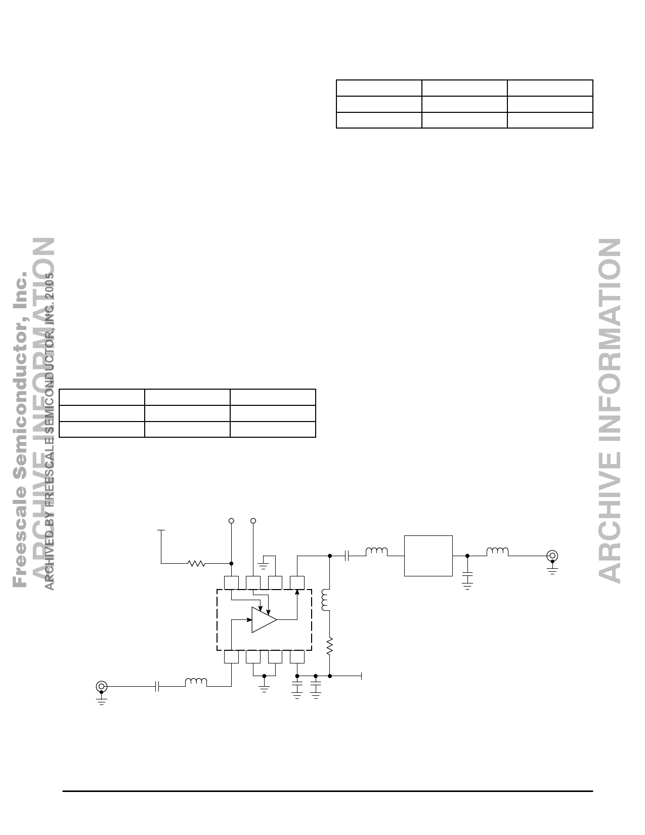
926.5 MHz Application Circuit, a ceramic deielectric filter
is used (Toko part # 4DFA–926A10).
LNA Input/Output
The LNA input impedance is the base of a common emitter
cascode amplifier. The LNA output is the collector of the
cascode stage and it is loaded with a series resistor of 400 Ω
and a capacitor of 10 pF to provide stability.
Digitally Programmable Bias/Enable
The LNA is enabled by a 2 bit (En1 and En2)
programmable bias circuit. The internal circuit shows the
comparator circuit which programs the internal regulator. The
logic table below shows the bias and typical performance.
ÁÁÁÁÁÁÁÁÁÁÁÁÁÁÁÁÁ f = 900 mHz
ÁÁÁÁÁÁÁÁÁÁÁÁÁÁÁÁÁ ICC/Gain
ÁÁÁÁÁÁÁÁÁÁÁÁÁÁÁÁÁ En1 Low
ÁÁÁÁÁÁÁÁÁÁÁÁÁÁÁÁÁÁÁÁÁÁÁÁÁÁÁÁÁÁÁÁÁÁÁÁÁÁÁÁÁÁÁÁÁÁÁÁÁÁÁ En1 High
En2 Low
0 mA/–22 dB
3.4 mA/13 dB
En2 High
1.2 mA/9.2 dB
8.2 mA/17 dB
Input/Output Matching
A typical application at 900 MHz yields 17 dB gain and
1.4 dB noise figure. In this circuit a series inductor of 5.6 nH
is used to match the input and a shunt inductor of 8.2 nH
which also serves as an RFC and a series capacitor of 0.9 p
is used to match the LNA output to 50 Ω load impedance.
It may be desirable to use a RF ceramic or SAW filter after
the LNA when driving a mixer to provide image frequency
rejection. The image filter is selected based on cost, size and
performance tradeoffs. Typical RF filters have 3.0 to 5.0 dB
insertion loss. Interface matching between the RF input, RF
filter and the mixer is shown in Application Circuit and the
Component Placement View.
A typical application at 1900 MHz yields 13 dB gain and
2.7 dB noise figure. In this circuit a series inductor of 5.6 nH
and a series capacitor of 1.0 pF are used to match the input
and a shut inductor of 2.0 nH and a series capacitor of 2.0 pF
are used to match the LNA output to 50 Ω load impedance.
Figure 2. MC13144D Application Circuit
(926.5 MHz)
En1 En2
VCC
1.0 M
8 765
100 p 39 nH
8.2 nH
Toko
Ceramic
Filter
8.2 nH
0.4 p
RF
Output
MC13144D
47
12 34
RF
47 p
Input
5.6 nH
100 n
100 p
VCC
4
For More Information On This Product, MOTOROLA RF/IF DEVICE DATA
Go to: www.freescale.com
Share Link: 