MC145507 데이터 시트보기 (PDF) - Motorola => Freescale
부품명
상세내역
제조사
MC145507 Datasheet PDF : 24 Pages
| |||
Freescale Semiconductor, Inc.
of 1.0, such that a 3 dBm0 signal at TxI corresponds to the
peak converter reference voltage as described in the Vref
and RSI pin descriptions. For a 3.15 V reference, the 3 dBm0
input should be 6.3 V peak–to–peak.
+Tx / –Tx
Positive Tx Amplifier Input
Negative Tx Amplifier Input
The Txl pin is the input to the transmit band–pass filter. If
+Tx or –Tx is available, then there is an internal amplifier
preceding the filter whose pins are +Tx, –Tx, and TxI. These
pins allow access to the amplifier terminals to tailor the input
gain with external resistors. The resistors should be in the
range of 10 kΩ.
POWER SUPPLIES
VDD
Most Positive Power Supply
VDD is typically 5 V to 12 V.
VSS
Most Negative Power Supply
VSS is typically 10 V to 12 V negative of VDD.
For a ±5 V dual–supply system, the typical power supply
configuration is VDD = 5 V, VSS = –5 V, VLS = 0 V (digital
ground accommodating TTL logic levels), and VAG = 0 V
being tied to system analog ground.
For single–supply applications, typical power supply con-
figurations include:
VDD = 10 V to 12 V
VSS = 0 V
VAG generates a mid supply voltage for referencing all ana-
log signals.
VLS controls the logic levels. This pin should be connected
to VDD for CMOS logic levels from VSS to VDD. This pin
should be connected to digital ground for true TTL logic input
levels referenced to VLS, with HCMOS output levels from VLS
to VDD.
TESTING CONSIDERATIONS (MC145506 ONLY)
An analog test mode is activated by connecting MSI and
CCI to 128 kHz. In this mode, the input of the A/D (the output
of the Tx filter) is available at the PDI pin. This input is direct
coupled to the A/D side of the codec. The A/D is a differential
design. This results in the gain of this input being effectively
attenuated by half. If monitored with a high–impedance buff-
er, the output of the Tx low–pass filter can also be measured
at the PDI pin. This test mode allows independent evaluation
of the transmit low–pass filter and A/D side of the codec. The
transmit and receive channels of these devices are tested
with the codec–filter fully functional.
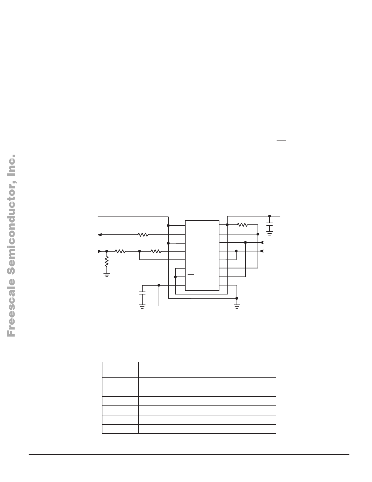
VAG
600 Ω
Rx
5 kΩ
Tx
10 kΩ
681
0.1 µF
MC145507
1 VAG
VDD 16
2
RxO
3 +Tx
15
RDD
RCE 14
4 TxI
RDC 13
5
–Tx
6
Mu/A
12
TDC
11
TDD
7 PDI
TDE 10
8 VSS
VLS 9
51 kΩ*
–5 V
* To define RDD when TDD is high Z.
Figure 1. Test Circuit
5V
0.1 µF
ENABLE
CLOCK
Table 1. MC145506 Options Available by Pin Selection
RSI*
Pin Level
Vref*
Pin Level
Peak–to–Peak Overload Voltage
(Txl, RxO)
VDD
VSS
7.56 Vp–p
VDD
VAG + VEXT
(3.02 x VEXT) Vp–p
VAG
VSS
5 Vp–p
VAG
VAG + VEXT
(2 x VEXT) Vp–p
VSS
VSS
6.3 Vp–p
VSS
VAG + VEXT
(2.52 x VEXT) Vp–p
* On MC145507/08, RSI and Vref are tied internally to VSS.
MC145506•MC145507•MC14550F8or More Information On This Product,
10
Go to: www.freescale.com
MOTOROLA
Share Link: 