MC145506 데이터 시트보기 (PDF) - Motorola => Freescale
부품명
상세내역
제조사
MC145506 Datasheet PDF : 24 Pages
| |||
Freescale Semiconductor, Inc.
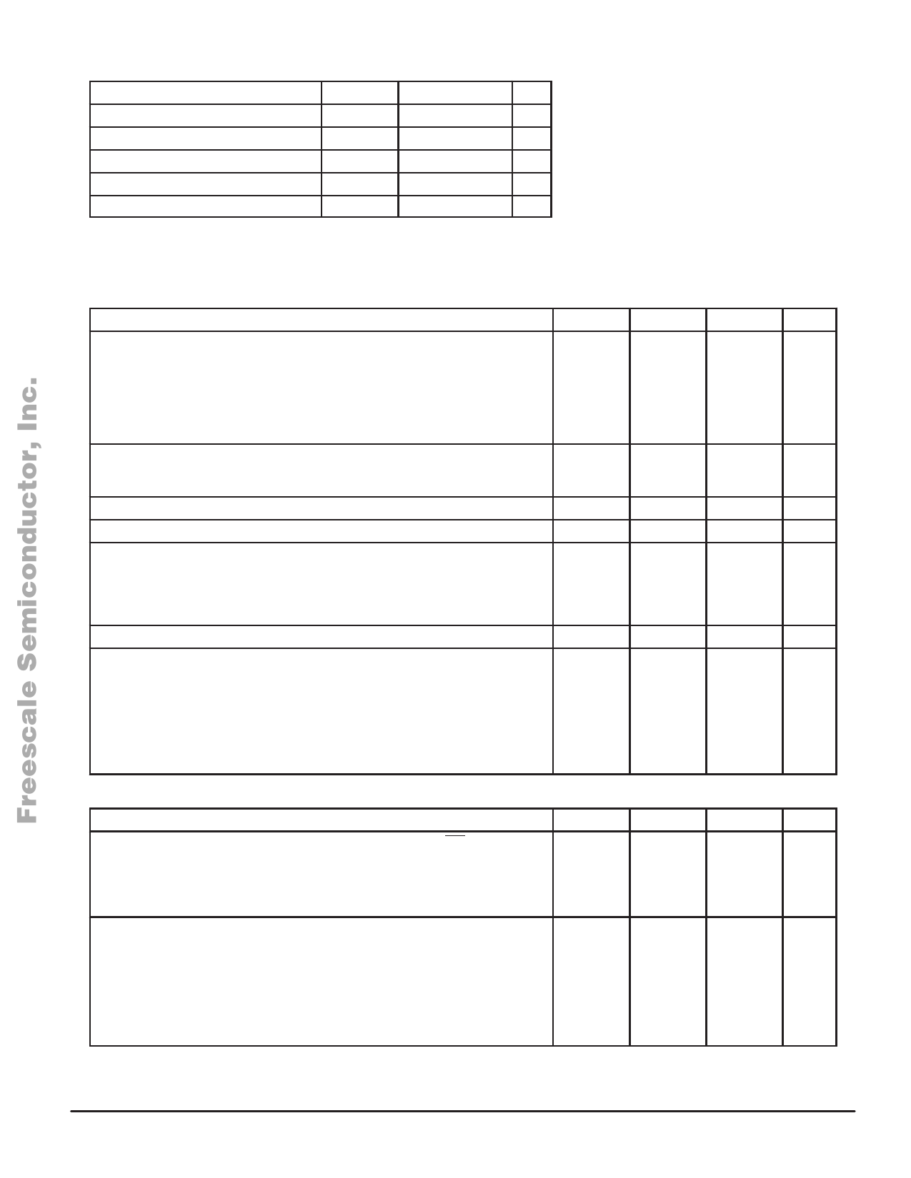
ABSOLUTE MAXIMUM RATINGS (Voltage Referenced to VSS)
Rating
Symbol
Value
Unit
DC Supply Voltage
VDD – VSS
–0.5 to 13
V
Voltage, Any Pin to VSS
V
–0.5 to VDD + 0.5 V
DC Drain Per Pin (Excluding VDD, VSS)
I
10
mA
Operating Temperature Range
TA
–40 to 85
°C
Storage Temperature Range
Tstg
–85 to 150
°C
This device contains circuitry to protect
against damage due to high static voltages or
electric fields; however, it is advised that
normal precautions be taken to avoid applica-
tion of any voltage higher than maximum rated
voltages to this high–impedance circuit. For
proper operation, it is recommended that Vin
and Vout be constrained to the range VSS ≤
(Vin or Vout) ≤ VDD.
Unused inputs must always be tied to an
appropriate logic voltage level (e.g., VSS,
VDD, VLS, or VAG).
RECOMMENDED OPERATING CONDITIONS (TA = –40° to 85°C)
Characteristic
Min
Typ
Max
Unit
DC Supply Voltage
Dual Supplies: VDD = –VSS (VAG = VLS = 0 V)
Single Supply: VDD to VSS (VAG is an Output, VLS = VDD or VSS)
MC145506, MC145507, MC145508 Using Internal 3.15 V Reference
MC145506 Using Internal 2.5 V Reference
MC145506 Using Internal 3.78 V Reference
MC145506 Using External 1.5 V Reference, Referenced to VAG
Power Dissipation
CMOS Logic Mode (VDD to VSS = 10 V, VLS = VDD)
HCMOS Logic Mode (VDD = 5 V, VSS = –5 V, VLS = VAG = 0 V)
Power Down Dissipation
4.75
5.0
V
6.3
8.5
—
12.6
7.0
—
12.6
9.5
—
12.6
4.75
—
12.6
mW
—
40
70
—
50
90
—
0.1
1.0
mW
Frame Rate Transmit and Receive
7.5
8.0
8.5
kHz
CCI Clock Rate (TDC Clock Rate for MC145507)
—
128
—
kHz
MC145506, MC145508
—
1536
—
Must Use One of These Frequencies ±2%, Relative to MSI Frequency of 8 kHz
—
1544
—
—
2048
—
—
2560
—
Data Rate for MC145506, MC145508
64
—
4096
kHz
Full Scale Analog Input and Output Level
MC145507, MC145508
VP
—
3.15
—
MC145506 (Vref = VSS)
RSI = VDD
—
3.78
—
RSI = VSS
—
3.15
—
RSI = VAG
—
2.5
—
MC145506 Using an External Reference Voltage Applied at Vref Pin RSI = VDD
—
1.51 x Vref
—
RSI = VSS
—
1.26 x Vref
—
RSI = VAG
—
Vref
—
DIGITAL LEVELS (VSS to VDD = 4.75 V to 12.6 V, TA = –40° to 85°C)
Characteristic
Symbol
Min
Max
Unit
Input Voltage Levels (TDE, TDC, RCE, RDC, RDD, DC, MSI, CCI, PDI)
CMOS Mode (VLS = VDD, VSS is Digital Ground)
HCMOS Mode (VLS ≤ VDD – 4.0 V, VLS is Digital Ground)
V
“0”
VIL
—
0.3 x VDD
“1”
VIH
0.7 x VDD
—
“0”
VIL
—
VLS + 0.8 V
“1”
VIH
VLS + 2.0 V
—
Output Current for TDD (Transmit Digital Data)
CMOS Mode (VLS = VDD, VSS = 0 V and is Digital Ground)
(VDD = 5 V, Vout = 0.4 V)
IOL
1.6
(VDD = 10 V, Vout = 0.5 V)
1.6
(VDD = 5 V, Vout = 4.5 V)
IOH
–1.6
(VDD = 10 V, Vout = 9.5 V)
–1.6
HCMOS Mode (VLS ≤ VDD – 4.75 V, VLS = 0 V and is Digital Ground) (VOL = 0.4 V)
IOL
1.6
(VOH = VDD – 0.5 V)
IOH
–1.6
mA
—
—
—
—
—
—
MOTOROLA
For More Information On This ProducMt,C145506•MC145507•MC145508
Go to: www.freescale.com
3
Share Link: 