MC1496B 데이터 시트보기 (PDF) - ON Semiconductor
부품명
상세내역
제조사
MC1496B Datasheet PDF : 14 Pages
| |||
MC1496, MC1496B
be introduced with or without modulation, provided its level
is sufficiently high to saturate the upper quad differential
amplifier. If the carrier signal is modulated, a 300 mVrms
input level is recommended.
Doubly Balanced Mixer
The MC1496 may be used as a doubly balanced mixer
with either broadband or tuned narrow band input and output
networks.
The local oscillator signal is introduced at the carrier input
port with a recommended amplitude of 100 mVrms.
Figure 29 shows a mixer with a broadband input and a
tuned output.
Frequency Doubler
The MC1496 will operate as a frequency doubler by
introducing the same frequency at both input ports.
Figures 30 and 31 show a broadband frequency doubler
and a tuned output very high frequency (VHF) doubler,
respectively.
Phase Detection and FM Detection
The MC1496 will function as a phase detector. High−level
input signals are introduced at both inputs. When both inputs
are at the same frequency the MC1496 will deliver an output
which is a function of the phase difference between the two
input signals.
An FM detector may be constructed by using the phase
detector principle. A tuned circuit is added at one of the
inputs to cause the two input signals to vary in phase as a
function of frequency. The MC1496 will then provide an
output which is a function of the input signal frequency.
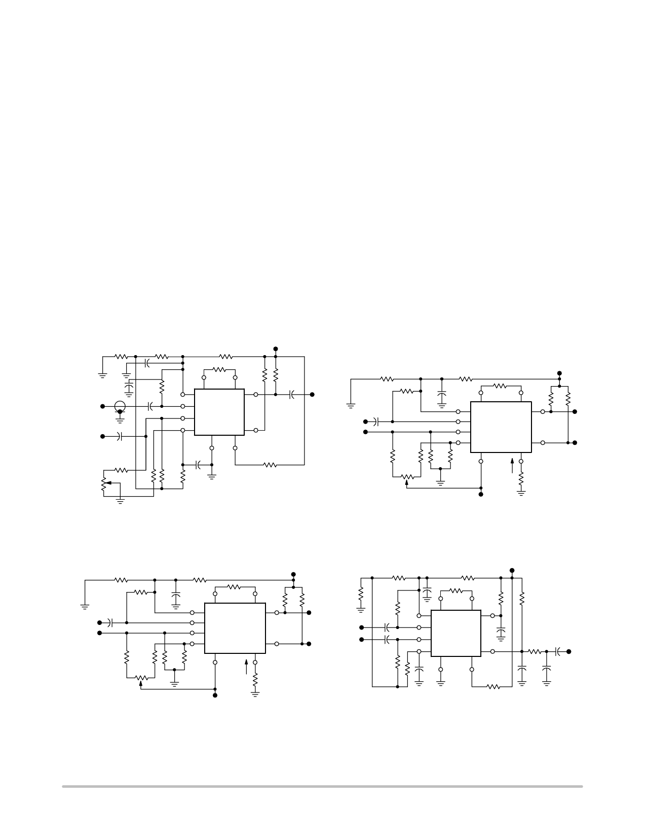
TYPICAL APPLICATIONS
1.0 k
820
VCC
1.3 k
12 Vdc
25 mF+
Carrier Input15 V
60 mVrms
0.1 mF
51
0.1 mF
Modulating − +
Signal Input 10 mF
300 mVrms 15 V
Carrier
Null 50 k
10 k 10 k
100
2 1.0 k
3.0 k
3
8
3.0 k
DSB
1.0 k
10
6
1 MC1496
4
25 mF 14
5 12
+15 V−
100
0.1 mF Output
51
VC 0.1 mF
Carrier
Input
VS
Modulating
10 k
Signal 10 k 10 k
Input
50 k
R1
Carrier Null
1.0 k
0.1 mF 2
8
10
1
4
51 51 14
Re 1.0 k
MC1496
I5
VEE
−8.0 Vdc
RL
3 3.9 k
6
12
5
6.8 k
VCC
12 Vd
RL
3.9
+
−
Figure 25. Balanced Modulator
(12 Vdc Single Supply)
Figure 26. Balanced Modulator−Demodulator
1.0 k
1.0 k
51
VC 0.1 mF
Carrier
Input VS
Modulating
Signal 750 750
Input
50 k
0.1 mF 2
8
10
1
4
51 51 14
Carrier Adjust
Re 1.0 k
MC1496
15
VEE
−8.0 Vdc
RL
3 3.9 k
6
12
5
6.8 k
VCC
12 Vdc
RL
1.0 k
3.9 k
+Vo Carrier Input
300 mVrms
SSB Input
−Vo
820
1.3 k
0.1 mF
51 8
0.1 mF
10
2 100 3 3.0 k
6
1 MC1496
0.1 mF 1.0 k
1.0 k
4
0.1 14
mF
5 12
10 k
VCC
12 Vdc
3.0 k
0.005
mF
1.0 k
1.0 mFOuAtFp
RLq 10
0.005 0.005
mF mF
Figure 27. AM Modulator Circuit
Figure 28. Product Detector
(12 Vdc Single Supply)
http://onsemi.com
10
Share Link: 