MC33201 데이터 시트보기 (PDF) - ON Semiconductor
부품명
상세내역
제조사
MC33201 Datasheet PDF : 19 Pages
| |||
MC33201, MC33202, MC33204, NCV33202, NCV33204
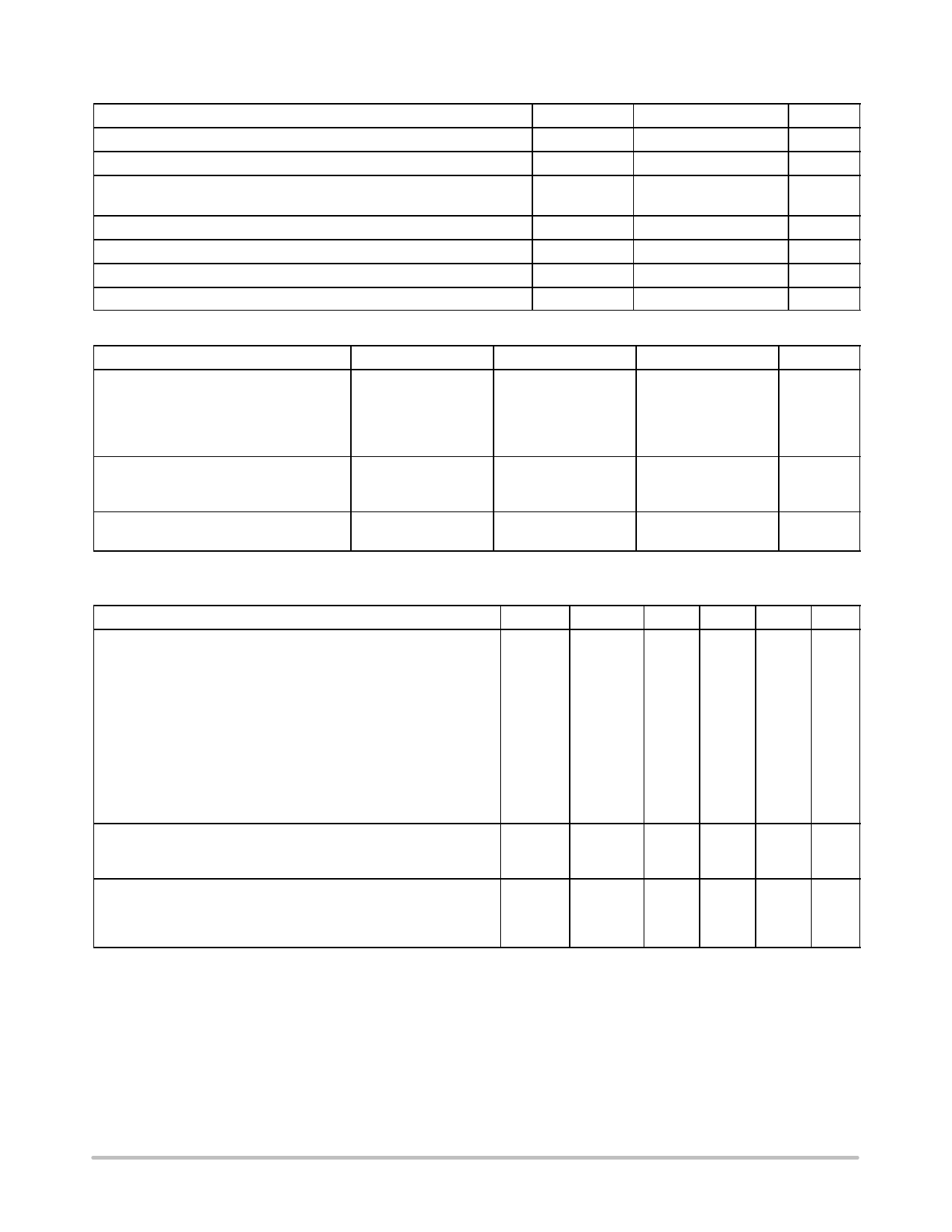
MAXIMUM RATINGS
Rating
Supply Voltage (VCC to VEE)
Input Differential Voltage Range
Common Mode Input Voltage Range (Note 2)
Output Short Circuit Duration
Maximum Junction Temperature
Storage Temperature
Maximum Power Dissipation
Symbol
VS
VIDR
VCM
ts
TJ
Tstg
PD
Value
Unit
+13
V
Note 1
V
VCC + 0.5 V to
V
VEE − 0.5 V
Note 3
sec
+150
°C
− 65 to +150
°C
Note 3
mW
DC ELECTRICAL CHARACTERISTICS (TA = 25°C)
Characteristic
VCC = 2.0 V
Input Offset Voltage
VIO (max)
MC33201
MC33202, NCV33202
MC33204, NCV33204
± 8.0
±10
±12
VCC = 3.3 V
± 8.0
±10
±12
Output Voltage Swing
VOH (RL = 10 kW)
VOL (RL = 10 kW)
1.9
3.15
0.10
0.15
Power Supply Current
per Amplifier (ID)
1.125
1.125
Specifications at VCC = 3.3 V are guaranteed by the 2.0 V and 5.0 V tests. VEE = GND.
VCC = 5.0 V
± 6.0
± 8.0
±10
4.85
0.15
1.125
Unit
mV
Vmin
Vmax
mA
DC ELECTRICAL CHARACTERISTICS (VCC = + 5.0 V, VEE = Ground, TA = 25°C, unless otherwise noted.)
Characteristic
Figure Symbol
Min
Typ
Max Unit
Input Offset Voltage (VCM 0 V to 0.5 V, VCM 1.0 V to 5.0 V)
MC33201: TA = + 25°C
MC33201: TA = − 40° to +105°C
MC33201V: TA = − 55° to +125°C
MC33202: TA = + 25°C
MC33202: TA = − 40° to +105°C
MC33202V: TA = − 55° to +125°C
NCV33202V: TA = − 55° to +125°C (Note 4)
MC33204: TA = + 25°C
MC33204: TA = − 40° to +105°C
MC33204V: TA = − 55° to +125°C
NCV33204: TA = − 55° to +125°C
3
⎮VIO⎮
mV
−
−
6.0
−
−
9.0
−
−
13
−
−
8.0
−
−
11
−
−
14
−
−
14
−
−
10
−
−
13
−
−
17
−
−
17
Input Offset Voltage Temperature Coefficient (RS = 50 W)
TA = − 40° to +105°C
TA = − 55° to +125°C
4
DVIO/DT
mV/°C
−
2.0
−
−
2.0
−
Input Bias Current (VCM = 0 V to 0.5 V, VCM = 1.0 V to 5.0 V)
TA = + 25°C
TA = − 40° to +105°C
TA = − 55° to +125°C
5, 6
⎮IIB⎮
nA
−
80
200
−
100
250
−
−
500
Stresses exceeding Maximum Ratings may damage the device. Maximum Ratings are stress ratings only. Functional operation above the
Recommended Operating Conditions is not implied. Extended exposure to stresses above the Recommended Operating Conditions may affect
device reliability.
1. The differential input voltage of each amplifier is limited by two internal parallel back−to−back diodes. For additional differential input voltage
range, use current limiting resistors in series with the input pins.
2. The input common mode voltage range is limited by internal diodes connected from the inputs to both supply rails. Therefore, the voltage
on either input must not exceed either supply rail by more than 500 mV.
3. Power dissipation must be considered to ensure maximum junction temperature (TJ) is not exceeded. (See Figure 2)
4. NCV33202 and NCV33204 are qualified for automotive use.
http://onsemi.com
3
Share Link: 