NCV33274ADTBR2G 데이터 시트보기 (PDF) - ON Semiconductor
부품명
상세내역
제조사
NCV33274ADTBR2G
ON Semiconductor

NCV33274ADTBR2G Datasheet PDF : 16 Pages
| |||
MC33272A, MC33274A, NCV33272A, NCV33274A
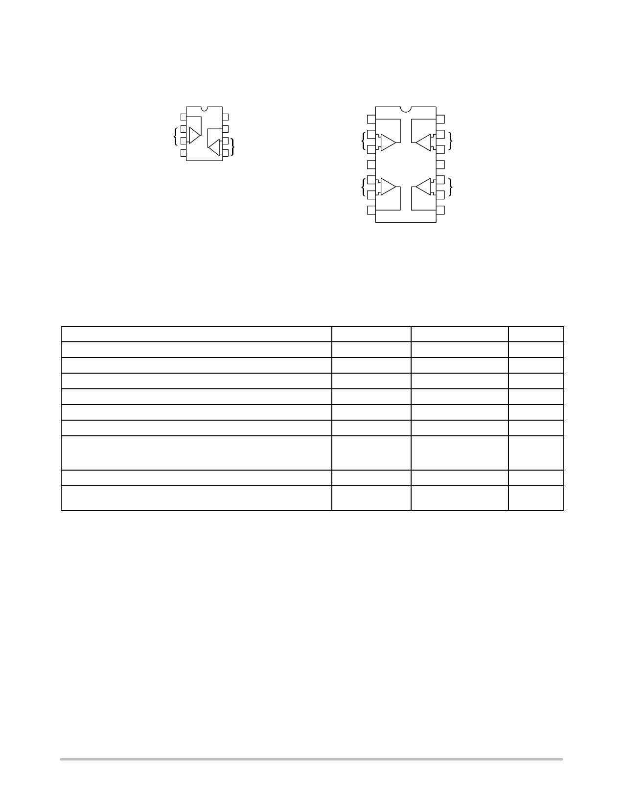
PIN CONNECTIONS
DUAL
CASE 626/751
Output 1 1
Inputs 1
2−
+
3
VEE 4
8 VCC
7 Output 2
−6
+5
Inputs 2
(Top View)
QUAD
CASE 646/751A/948G
Output 1 1
2
Inputs 1
−
3 +1
VCC 4
Inputs 2
5
6
+
−2
Output 2 7
14 Output 4
13
−
4 + 12
Inputs 4
11 VEE
+ 10
3− 9
Inputs 3
8 Output 3
(Top View)
MAXIMUM RATINGS
Rating
Symbol
Value
Unit
Supply Voltage
VCC to VEE
+36
V
Input Differential Voltage Range
VIDR
Note 1
V
Input Voltage Range
VIR
Note 1
V
Output Short Circuit Duration (Note 2)
Maximum Junction Temperature
Storage Temperature
tSC
Indefinite
sec
TJ
+150
°C
Tstg
−60 to +150
°C
ESD Protection at Any Pin
− Human Body Model
− Machine Model
Vesd
V
2000
200
Maximum Power Dissipation
Operating Temperature Range
PD
MC33272A, MC33274A
TA
NCV33272A, NCV33274A
Note 2
mW
−40 to +85
°C
−40 to +125
Stresses exceeding Maximum Ratings may damage the device. Maximum Ratings are stress ratings only. Functional operation above the
Recommended Operating Conditions is not implied. Extended exposure to stresses above the Recommended Operating Conditions may affect
device reliability.
1. Either or both input voltages should not exceed VCC or VEE.
2. Power dissipation must be considered to ensure maximum junction temperature (TJ) is not exceeded (see Figure 2).
http://onsemi.com
2
Share Link: