MC33560 데이터 시트보기 (PDF) - ON Semiconductor
부품명
상세내역
제조사
MC33560 Datasheet PDF : 26 Pages
| |||
MC33560
Table 1. PIN FUNCTION DESCRIPTION
Pin Symbol
Type
Name/Function
CARD INTERFACE
19 CRDC8
I/O
General purpose input/output. It has the same behavior as CRDIO. It can be connected to the
ÁÁÁÁÁÁÁÁÁÁÁÁÁÁÁÁÁÁÁÁÁÁÁÁÁÁÁÁÁÁÁÁÁÁÁÁÁÁÁÁÁÁÁÁÁÁÁÁÁÁÁÁÁÁÁÁÁÁÁÁÁÁÁÁÁÁ C8 pin of the card connector.
CURRENT LIMIT AND THERMAL PROTECTION
1 PGND
POWER
This pin is the return path for the current flowing into Pin 22 (L1). It must be connected to
CRDGND using appropriate grounding techniques.
12 CRDGND POWER
This pin is the signal ground. It must be connected to the ground pin of the card connector. It is
the reference level for all analog and digital signals.
13 CRDVCC
POWER
This pin connects to the VCC pin of the card connector. It is the reference level for a logic “1” of
Pins 11, 14, 15, 16 and 19.
22 L1
POWER
This pin connects to an external inductance for the DC−DC converter. Please refer to the
description of the DC−DC converter functional block.
23 VBAT
POWER
This pin is connected to the supply voltage. Logic level “1” of Pins 2 to 10, 17, 18, 20 and 21 is
referenced to VBAT. Operation of the MC33560 is inhibited when VBAT is lower than the
minimum value.
24 ILIM
POWER
This pin can be connected to the PGND pin, or to a resistor connected to PGND, or left open,
depending on the peak coil current needed to supply the card.
PROGRAMMING AND STATUS FUNCTIONS
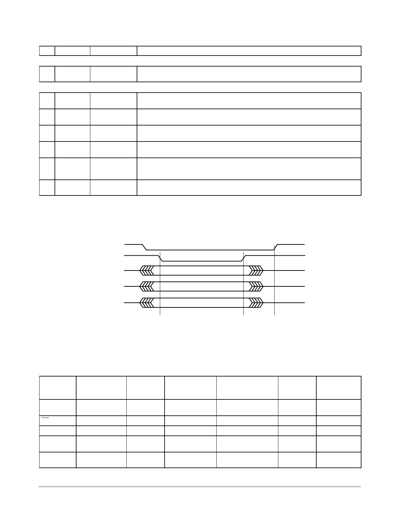
The MC33560 features a programming interface and a status interface. Figure 20 shows how to enter and exit programming
mode; Table 2 shows which pins are used to access the various functions.
RDYMOD (in)
CS
PWRON
PROGRAM DATA VALUE
RESET
PROGRAM DATA VALUE
IO
PROGRAM DATA VALUE
ENTER
PROGRAMMING
MODE
LATCH
EXIT
PROGRAM PROGRAMMING
VALUE
MODE
Figure 20. MC33560 Programming Sequence
Table 2. PIN USE FOR PROGRAMMING AND STATUS FUNCTIONS
Programs CRDV-
CC
TO 3 V/5 V
Select VCC
ON/OFF
Select
Clock Input
Program ASYCLKIN
Divide Ratio
RDYMOD
(In/Out)
Force to 0
READ
Force to 0
Force to 0
CS (In)
rising edge
0
rising edge
rising edge
PWRON
RESET(In)
0/1
Programs CLK
Input/Divide Ratio
0/1
NOT USED
Programs CRDVCC
0/1
Programs CRDVCC
0/1
I/O(In)
Programs CLK
NOT USED
0/1
0/1
Input/Divide Ratio
Poll Card
Status
READ
0
0 or Hi−z
NOT USED
NOT USED
Poll CRDVCC
Status
READ
0
1
NOT USED
NOT USED
http://onsemi.com
11
Share Link: 