MC74VHC50 데이터 시트보기 (PDF) - ON Semiconductor
부품명
상세내역
제조사
MC74VHC50 Datasheet PDF : 7 Pages
| |||
MC74VHC50
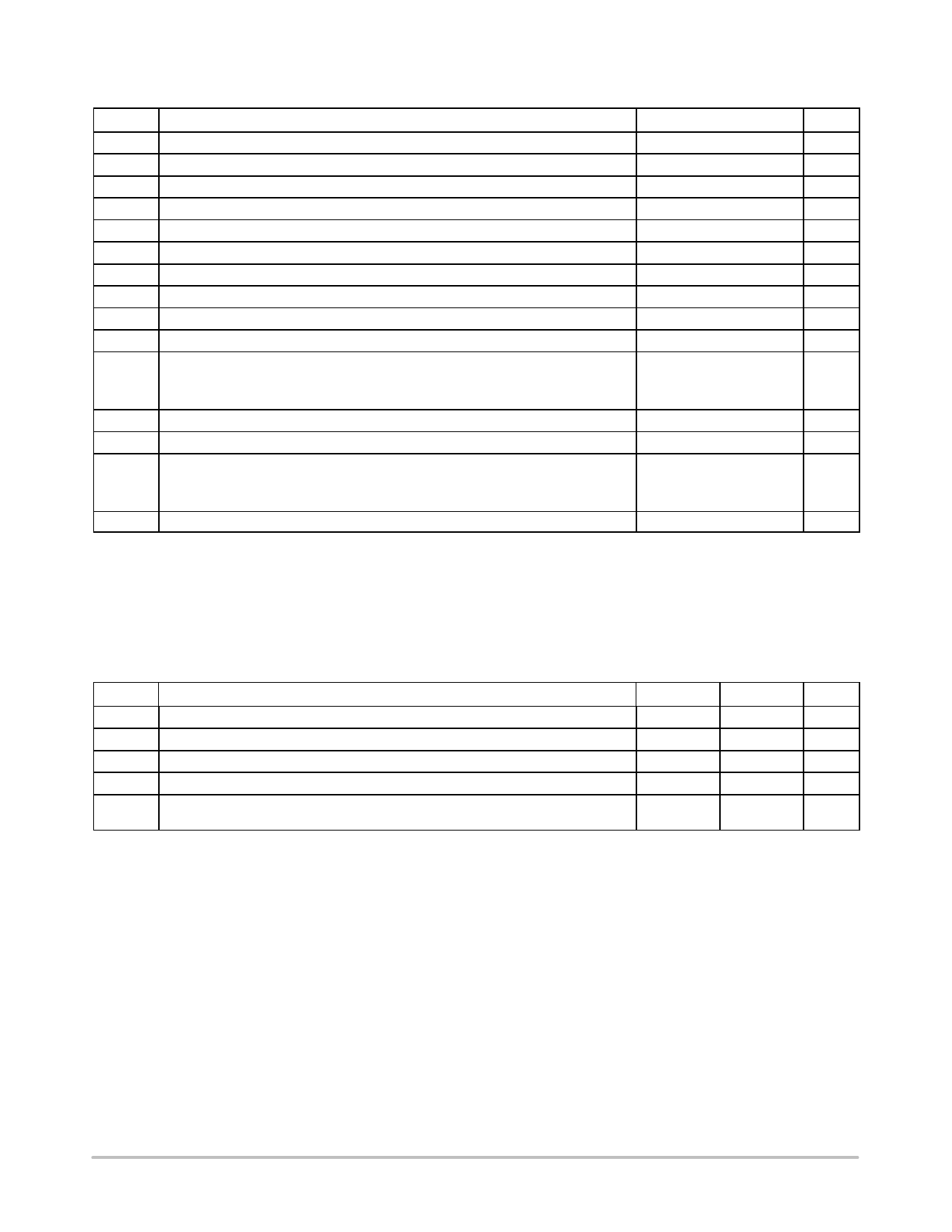
MAXIMUM RATINGS
Symbol
Parameter
Value
Unit
VCC
VIN
VOUT
IIK
IOK
IOUT
ICC
TSTG
TL
TJ
qJA
DC Supply Voltage
DC Input Voltage
DC Output Voltage
DC Input Diode Current
DC Output Diode Current
DC Output Sink Current
DC Supply Current per Supply Pin
Storage Temperature Range
Lead Temperature, 1 mm from Case for 10 Seconds
Junction Temperature under Bias
Thermal Resistance
VI < GND
VO < GND
(Note 1)
SOIC
TSSOP
*0.5 to )7.0
*0.5 to )7.0
*0.5 to VCC )0.5
*20
$20
$25
$50
*65 to )150
260
)150
125
170
V
V
V
mA
mA
mA
mA
°C
°C
°C
°C/W
MSL
Moisture Sensitivity
Level 1
FR
VESD
Flammability Rating
ESD Withstand Voltage
Oxygen Index: 30 to 35 UL 94 V−0 @ 0.125 in
Human Body Model (Note 2)
> 2000
V
Machine Model (Note 3)
> 200
Charged Device Model (Note 4)
2000
ILatch−Up Latch−Up Performance
Above VCC and Below GND at 85°C (Note 5)
$300
mA
Stresses exceeding Maximum Ratings may damage the device. Maximum Ratings are stress ratings only. Functional operation above the
Recommended Operating Conditions is not implied. Extended exposure to stresses above the Recommended Operating Conditions may affect
device reliability.
1. Measured with minimum pad spacing on an FR4 board, using 10 mm−by−1 inch, 2−ounce copper trace with no air flow.
2. Tested to EIA/JESD22−A114−A.
3. Tested to EIA/JESD22−A115−A.
4. Tested to JESD22−C101−A.
5. Tested to EIA/JESD78.
RECOMMENDED OPERATING CONDITIONS
Symbol
Parameter
Min
Max
Unit
VCC
Supply Voltage
2.0
5.5
V
VI
Input Voltage
(Note 6)
0
5.5
V
VO
Output Voltage
(HIGH or LOW State)
0
VCC
V
TA
Operating Free−Air Temperature
*55
)125
°C
Dt/DV
Input Transition Rise or Fall Rate
VCC = 3.0 V $0.3 V
0
VCC = 5.0 V $0.5 V
0
100
ns/V
20
6. Unused inputs may not be left open. All inputs must be tied to a high− or low−logic input voltage level.
NOTE: The qJA of the package is equal to 1/Derating. Higher junction temperatures may affect the expected lifetime of the device per the table
and figure below.
http://onsemi.com
2
Share Link: 