CXD1170 데이터 시트보기 (PDF) - Sony Semiconductor
부품명
상세내역
제조사
CXD1170 Datasheet PDF : 8 Pages
| |||
CXD1170M
Absolute Maximum Ratings (Ta = 25°C)
• Supply voltage
VDD
7
V
• Input voltage
VIN
VDD to VSS
V
• Output current
IOUT
15
mA
• Storage temperature
Tstg
–55 to +150
°C
Recommended Operating Conditions
• Supply voltage
AVDD, AVSS
4.75 to 5.25
V
DVDD, DVSS
4.75 to 5.25
V
• Reference input voltage VREF
2.0
V
• Clock pulse width
Tpw1
12.5 (Min)
ns
Tpw0
12.5 (Min)
ns
• Operating temperature Topr
–20 to +75
°C
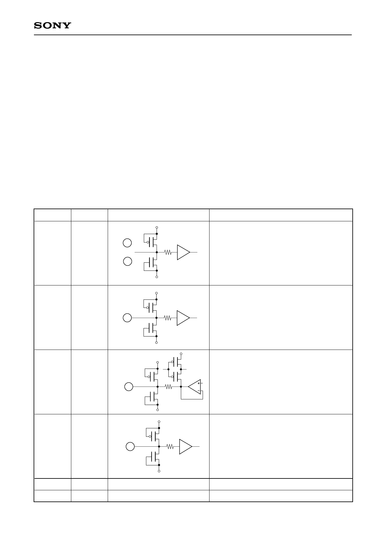
Pin Description and I/O Pins Equivalent Circuit
No.
Symbol
Equivalent circuit
DVDD
3
3 to 8 D0 to D5
to
8
DVSS
DVDD
9
BLK
9
11
VB
DVSS
DVDD
DVDD
11
Description
Digital input
Blanking pin
No signal at "H" (Output 0V)
Output condition at "L"
Connect a capacitor of about 0.1µF
12
CLK
10, 13
14
DVSS
AVSS
DVSS
DVDD
12
DVSS
Clock pin
Moreover all input pins are TTL-CMOS
compatible
Digital GND
Analog GND
–2–
Share Link: 