MOC8204 데이터 시트보기 (PDF) - Motorola => Freescale
부품명
상세내역
제조사
MOC8204 Datasheet PDF : 6 Pages
| |||
MOC8204 MOC8205 MOC8206
ELECTRICAL CHARACTERISTICS (TA = 25°C unless otherwise noted)(1)
Characteristic
Symbol
Min
INPUT LED (TA = 25°C unless otherwise noted)
Reverse Leakage Current
(VR = 6 V)
Forward Voltage
(IF = 10 mA)
Capacitance
(V = 0 V, f = 1 MHz)
IR
—
VF
—
CJ
—
OUTPUT TRANSISTOR (TA = 25°C and IF = 0 unless otherwise noted)
Collector–Emitter Dark Current (RBE = 1 MΩ)
(VCE = 300 V)
TA = 25°C
TA = 100°C
ICER
—
—
Collector–Base Breakdown Voltage
(IC = 100 µA)
V(BR)CBO
400
Collector–Emitter Breakdown Voltage
(IC = 1 mA, RBE = 1 MΩ)
V(BR)CER
400
Emitter–Base Breakdown Voltage
(IE = 100 µA)
V(BR)EBO
7
COUPLED (TA = 25°C unless otherwise noted)
Output Collector Current
(VCE = 10 V, IF = 10 mA, RBE = 1 MΩ)
MOC8204
MOC8205
MOC8206
IC (CTR)(2)
2 (20)
1 (10)
0.5 (5)
Collector–Emitter Saturation Voltage
(IC = 0.5 mA, IF = 10 mA, RBE = 1 MΩ)
Surge Isolation Voltage (Input to Output)(3)
Peak ac Voltage, 60 Hz, 1 sec
Isolation Resistance(3 )
(V = 500 V)
Isolation Capacitance(1)
(V = 0 V, f = 1 MHz)
VCE(sat)
VISO
RISO
CISO
—
7500
—
—
Turn–On Time
Turn–Off Time
VCC = 10 V, IC = 2 mA, RL = 100 Ω
ton
—
toff
—
1. Always design to the specified minimum/maximum electrical limits (where applicable).
2. Current Transfer Ratio (CTR) = IC/IF x 100%.
3. For this test LED Pins 1 and 2 are common and phototransistor Pins 4, 5 and 6 are common.
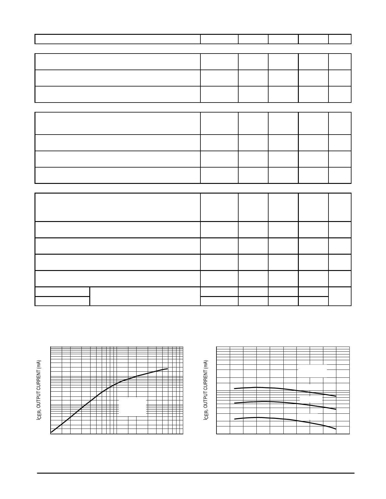
TYPICAL CHARACTERISTICS
Typ(1)
—
1.2
18
—
—
—
—
—
—
—
—
—
—
1011
0.2
5
5
Max
Unit
10
µA
15
Volts
—
pF
100
nA
250
µA
—
Volts
—
Volts
—
Volts
mA (%)
—
—
—
0.4
Volts
—
Vac(pk)
—
Ohms
—
pF
—
µs
—
50
20
10
5
2
RBE = 106 Ω
1
VCE = 10 V
0.5
TA = 25°C
0.2
0.1
1
2
5
10
20
50
IF, LED INPUT CURRENT (mA)
Figure 1. Output Current versus LED Input Current
RBE = 106 Ω
20
VCE = 10 V
10
IF = 20 mA
IF = 10 mA
5
IF = 5 mA
2
1
–60 –40 –20 0 20 40 60 80 100
TA, AMBIENT TEMPERATURE (°C)
Figure 2. Output Current versus Temperature
2
Motorola Optoelectronics Device Data
Share Link: 