MCP1702 데이터 시트보기 (PDF) - Microchip Technology
부품명
상세내역
제조사
MCP1702 Datasheet PDF : 26 Pages
| |||
MCP1702
1.0 ELECTRICAL
CHARACTERISTICS
Absolute Maximum Ratings †
VDD...............................................................................+14.5V
All inputs and outputs w.r.t. .............(VSS-0.3V) to (VIN+0.3V)
Peak Output Current ...................................................500 mA
Storage temperature .....................................-65°C to +150°C
Maximum Junction Temperature ................................... 150°C
ESD protection on all pins (HBM;MM) 4 kV; 400V
† Notice: Stresses above those listed under “Maximum
Ratings” may cause permanent damage to the device. This is
a stress rating only and functional operation of the device at
those or any other conditions above those indicated in the
operational listings of this specification is not implied.
Exposure to maximum rating conditions for extended periods
may affect device reliability.
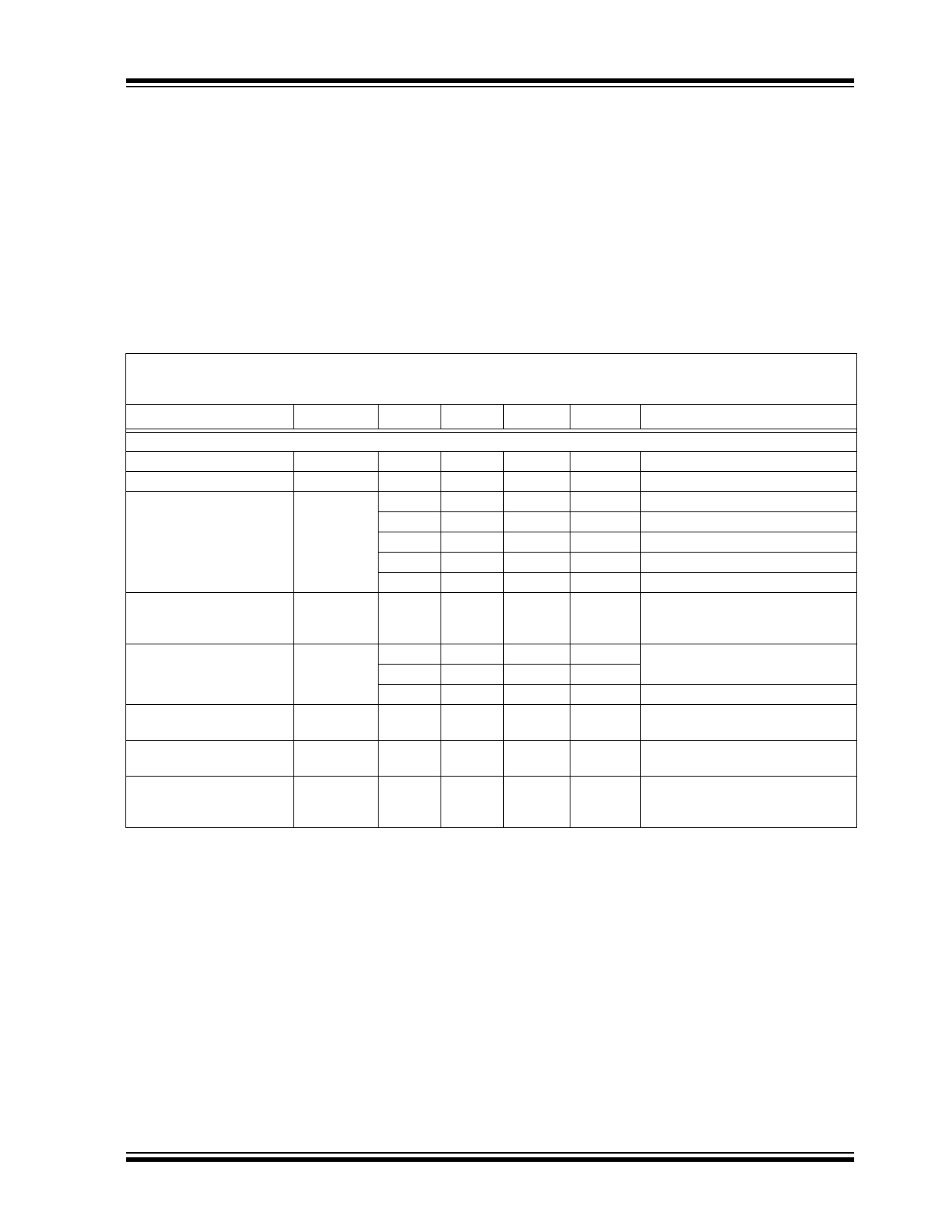
DC CHARACTERISTICS
Electrical Specifications: Unless otherwise specified, all limits are established for VIN = VOUT(MAX) + VDROPOUT(MAX), Note 1,
ILOAD = 100 µA, COUT = 1 µF (X7R), CIN = 1 µF (X7R), TA = +25°C.
Boldface type applies for junction temperatures, TJ of -40°C to +125°C. (Note 7)
Parameters
Sym
Min
Typ
Max
Units
Conditions
Input / Output Characteristics
Input Operating Voltage
VIN
2.7
—
13.2
Input Quiescent Current
Iq
—
2.0
5
Maximum Output Current
IOUT_mA
250
—
—
50
100
—
100
130
—
150
200
—
200
250
—
Output Short Circuit Current
IOUT_SC
—
400
—
V
Note 1
µA
IL = 0 mA
mA
For VR 2.5V
mA
For VR < 2.5V, VIN 2.7V
mA
For VR < 2.5V, VIN 2.95V
mA
For VR < 2.5V, VIN 3.2V
mA
For VR < 2.5V, VIN 3.45V
mA
VIN = VIN(MIN) (Note 1), VOUT = GND,
Current (average current) measured
10 ms after short is applied.
Output Voltage Regulation
VOUT
VR-3.0% VR±0.4% VR+3.0%
V
Note 2
VR-2.0% VR±0.4% VR+2.0%
V
VOUT Temperature
Coefficient
TCVOUT
VR-1.0% VR±0.4% VR+1.0%
—
50
—
V
1% Custom
ppm/°C Note 3
Line Regulation
VOUT/
-0.3
(VOUTXVIN)
±0.1
+0.3
%/V
(VOUT(MAX) + VDROPOUT(MAX))
VIN 13.2V, (Note 1)
Load Regulation
VOUT/VOUT
-2.5
±1.0
+2.5
%
IL = 1.0 mA to 250 mA for VR 2.5V
IL = 1.0 mA to 200 mA for VR 2.5V,
VIN = 3.45V (Note 4)
Note 1:
2:
3:
4:
The minimum VIN must meet two conditions: VIN2.7V and VIN VOUT(MAX) + VDROPOUT(MAX).
VR is the nominal regulator output voltage. For example: VR = 1.2V, 1.5V, 1.8V, 2.5V, 2.8V, 3.0V, 3.3V, 4.0V, or 5.0V. The
input voltage VIN = VOUT(MAX) + VDROPOUT(MAX) or VIN = 2.7V (whichever is greater); IOUT = 100 µA.
TCVOUT = (VOUT-HIGH - VOUT-LOW) *106 / (VR * Temperature), VOUT-HIGH = highest voltage measured over the
temperature range. VOUT-LOW = lowest voltage measured over the temperature range.
Load regulation is measured at a constant junction temperature using low duty cycle pulse testing. Changes in output
voltage due to heating effects are determined using thermal regulation specification TCVOUT.
5: Dropout voltage is defined as the input to output differential at which the output voltage drops 2% below its measured
value with an applied input voltage of VOUT(MAX) + VDROPOUT(MAX) or 2.7V, whichever is greater.
6: The maximum allowable power dissipation is a function of ambient temperature, the maximum allowable junction
temperature and the thermal resistance from junction to air (i.e., TA, TJ, JA). Exceeding the maximum allowable power
dissipation will cause the device operating junction temperature to exceed the maximum 150°C rating. Sustained
junction temperatures above 150°C can impact the device reliability.
7: The junction temperature is approximated by soaking the device under test at an ambient temperature equal to the
desired Junction temperature. The test time is small enough such that the rise in the Junction temperature over the
ambient temperature is not significant.
2010 Microchip Technology Inc.
DS22008E-page 3
Share Link: 