MCP1702 데이터 시트보기 (PDF) - Microchip Technology
부품명
상세내역
제조사
MCP1702 Datasheet PDF : 26 Pages
| |||
MCP1702
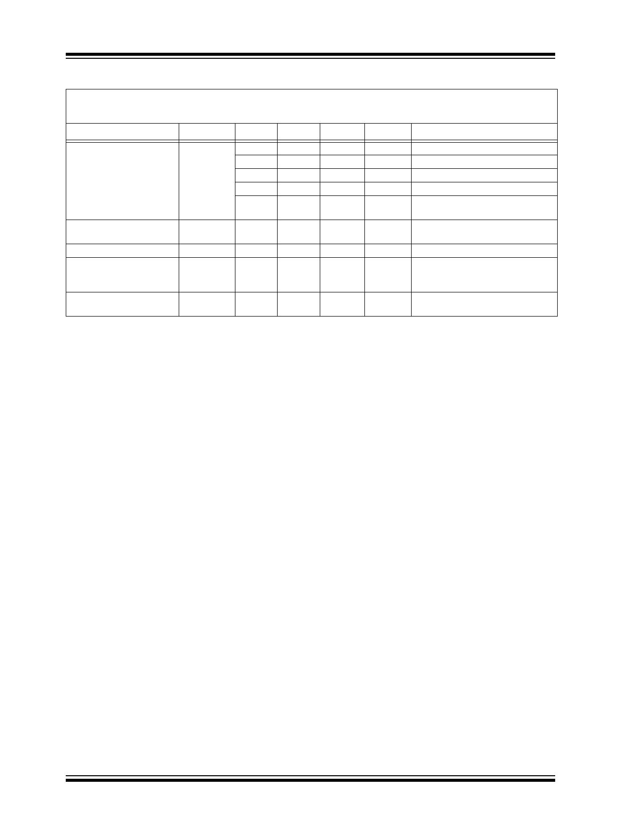
DC CHARACTERISTICS (CONTINUED)
Electrical Specifications: Unless otherwise specified, all limits are established for VIN = VOUT(MAX) + VDROPOUT(MAX), Note 1,
ILOAD = 100 µA, COUT = 1 µF (X7R), CIN = 1 µF (X7R), TA = +25°C.
Boldface type applies for junction temperatures, TJ of -40°C to +125°C. (Note 7)
Parameters
Sym
Min
Typ
Max
Units
Conditions
Dropout Voltage
(Note 1, Note 5)
VDROPOUT
—
—
—
—
—
330
650
525
725
625
975
750
1100
—
—
mV
IL = 250 mA, VR = 5.0V
mV
IL = 250 mA, 3.3V VR < 5.0V
mV
IL = 250 mA, 2.8V VR < 3.3V
mV
IL = 250 mA, 2.5V VR < 2.8V
mV
VR < 2.5V, See Maximum Output
Current Parameter
Output Delay Time
Output Noise
TDELAY
eN
—
1000
—
µs
VIN = 0V to 6V, VOUT = 90% VR
RL = 50 resistive
—
8
—
µV/(Hz)1/2 IL = 50 mA, f = 1 kHz, COUT = 1 µF
Power Supply Ripple
Rejection Ratio
PSRR
—
44
—
dB
f = 100 Hz, COUT = 1 µF, IL = 50 mA,
VINAC = 100 mV pk-pk, CIN = 0 µF,
VR = 1.2V
Thermal Shutdown
Protection
TSD
—
150
—
°C
Note 1:
2:
3:
4:
The minimum VIN must meet two conditions: VIN2.7V and VIN VOUT(MAX) + VDROPOUT(MAX).
VR is the nominal regulator output voltage. For example: VR = 1.2V, 1.5V, 1.8V, 2.5V, 2.8V, 3.0V, 3.3V, 4.0V, or 5.0V. The
input voltage VIN = VOUT(MAX) + VDROPOUT(MAX) or VIN = 2.7V (whichever is greater); IOUT = 100 µA.
TCVOUT = (VOUT-HIGH - VOUT-LOW) *106 / (VR * Temperature), VOUT-HIGH = highest voltage measured over the
temperature range. VOUT-LOW = lowest voltage measured over the temperature range.
Load regulation is measured at a constant junction temperature using low duty cycle pulse testing. Changes in output
voltage due to heating effects are determined using thermal regulation specification TCVOUT.
5: Dropout voltage is defined as the input to output differential at which the output voltage drops 2% below its measured
value with an applied input voltage of VOUT(MAX) + VDROPOUT(MAX) or 2.7V, whichever is greater.
6: The maximum allowable power dissipation is a function of ambient temperature, the maximum allowable junction
temperature and the thermal resistance from junction to air (i.e., TA, TJ, JA). Exceeding the maximum allowable power
dissipation will cause the device operating junction temperature to exceed the maximum 150°C rating. Sustained
junction temperatures above 150°C can impact the device reliability.
7: The junction temperature is approximated by soaking the device under test at an ambient temperature equal to the
desired Junction temperature. The test time is small enough such that the rise in the Junction temperature over the
ambient temperature is not significant.
DS22008E-page 4
2010 Microchip Technology Inc.
Share Link: 